AMD RX 9080 XT ES engineering sample could rival RTX 5080 Super
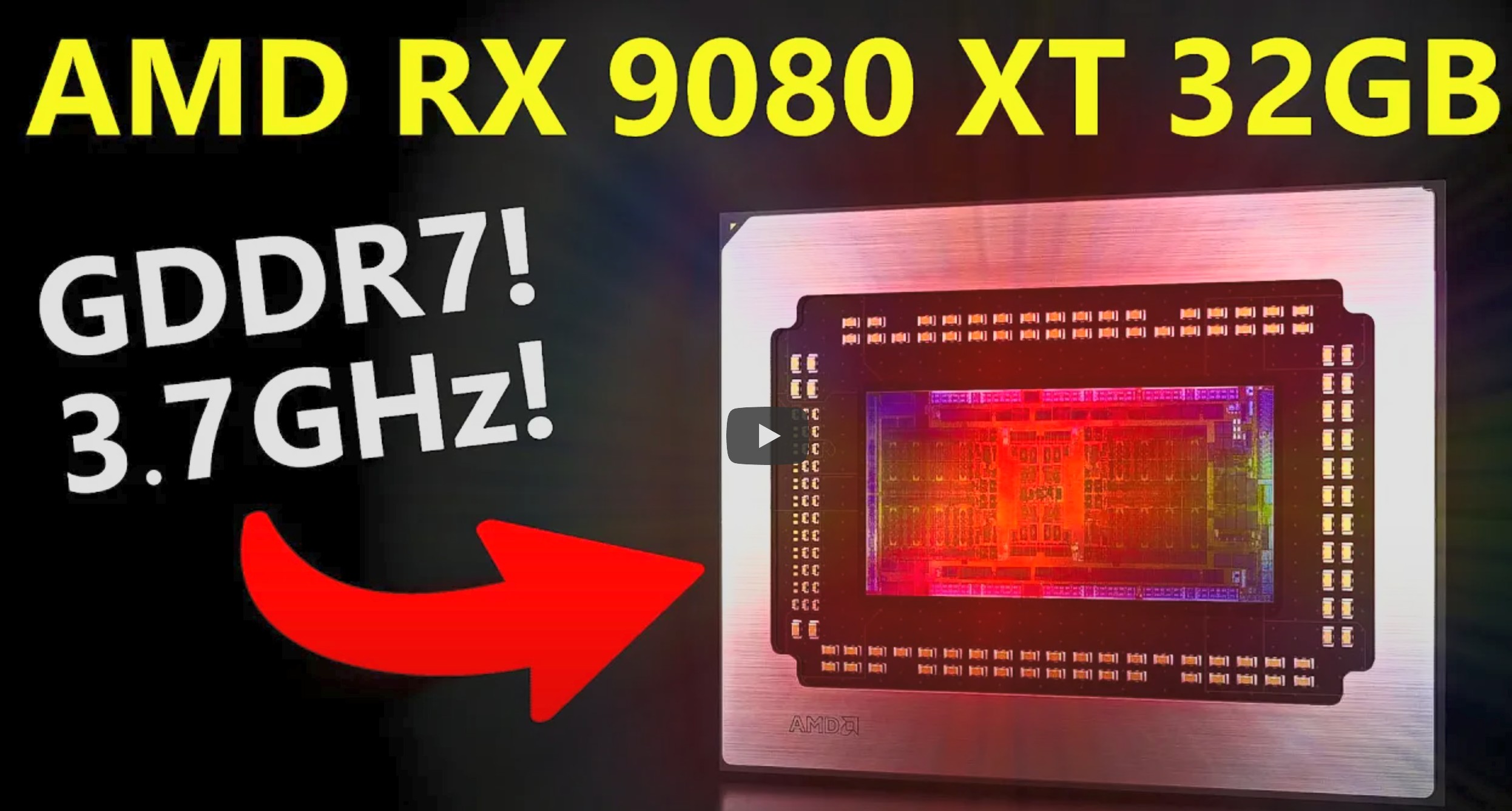
Internal AMD lab tests reportedly show the card running game clocks between 3.4 and 3.7 GHz. The GPU features a 256-bit GDDR7 memory interface and configurations with up to 32 GB of VRAM. Some samples also include 16 GB and 24 GB memory variants. In terms of power, the card is pushed well past 450 watts under load, with some units exceeding 500 watts in overclocked conditions.
According to early benchmark data shared confidentially with Moore's Law Is Dead, performance uplift at 4K resolution averages 28% over the RX 9070 XT, with peaks of up to 45% in certain workloads. This would place the RX 9080 XT ES in direct contention with the RTX 5080 Super and possibly even the RTX 4090, depending on implementation and final clock speeds. This is all speculative at this time.
The GPU, which may be based on a refined Navi 48 architecture, is not expected to use a radical redesign. Instead, AMD appears to be pursuing higher clocks and memory bandwidth within a traditional monolithic layout. It may also be leveraging TSMC's N4X or even N3X process nodes to achieve the reported performance. AMD has publicly confirmed a roadmap including N2X and 1.4 nm nodes for future CPUs, making the use of cutting-edge nodes plausible.
Moore's Law Is Dead speculates that the RX 9080 XT ES could follow a strategy similar to Radeon VII, which used a die-shrunk version of Vega to pre-empt NVIDIA's 7 nm transition. However, AMD has not confirmed any launch plans. The engineering sample may remain internal unless AMD identifies a market window or competitive pressure that justifies a release.
The final decision could hinge on the readiness of FSR4 (Redstone) and broader strategic considerations. Multiple sources suggest AMD may wait to combine a potential RX 9080 XT release with improved upscaling technology to deliver a fully competitive high-end product.
