Samsung formally launches 3nm chip production at a South Korean facility
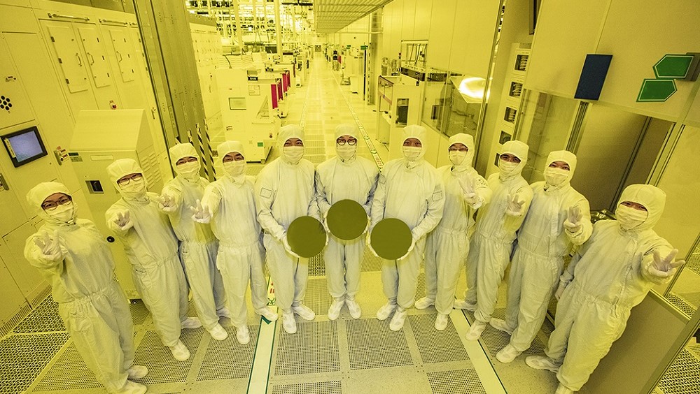
Samsung has finally made the leap to 3nm official, claiming to have successfully produced the first wafers for chips of this next-gen architecture at its Electronics division's Hwaseong campus in South Korea. 3nm is widely touted as the natural upgrade to the latest processors such as the Apple A15 Bionic or Qualcomm Snapdragon 8 Gen 1.
Samsung's breakthrough puts it ahead in the race to full-scale 3nm mass production, ahead of its rival TSMC. The OEM has now also confirmed that this will be done based on its in-house MBCFET, a patented version of the gate-all-around field-effect transistor (GAAFET).
MBCFETs are produced using the "nanosheet" process technique, which, according to Samsung, results in a final product with a surface area reduced by 16% compared to a 5nm counterpart thus far. This stat may set 3nm for increased yields; however, actual clients and users may be even more interested in initial claims of performance that could go up to 23% greater than the older node, while using up to 45% less energy.
That is just for first-gen 3nm, moreover, with Samsung also now projecting performance and power-efficiency gains of +35% and +50% respectively, while shrinking its surface area even further to 35% less compared to 5nm.
Despite these potential advantages, the OEM acknowledges that the upgrade to 3nm might make final chip design and integration even tougher and more complicated for its prospective clients.
To this end, the company has implemented Samsung Advanced Foundry Ecosystem (SAFE), an infrastructure solution developed alongside partners such as Synopsys, Siemens, Cadence and Ansys to make the ultimate steps in getting future 3nm-based devices onto the market.
Source(s)
