

Intel Core Ultra 5 245HX vs AMD Ryzen 7 H 260 vs Intel Core Ultra 7 265HX
Intel Core Ultra 5 245HX
► remove from comparisonThe Intel Core Ultra 5 245HX is a fast mid-range mobile CPU for gaming notebooks based on the Arrow Lake architecture. It offers 20 cores consisting of 6 of the 8 fast performance cores with up to 5.1 GHz and 8 of the 16 smaller efficiency cores with up to 4.5 GHz clock speed. The CPU can access 24 MB L2 cache and 26 MB L3 cache and is specified with a TDP of 55 watts.
The SoC integrates a small dedicated NPU called AI Boost with 13 TOPS (Int8) and optionally supports vPro Enterprise. The integrated memory controller supports up to 192 GB DDR5-6400 (dual channel, ECC optional). The integrated GPU (iGPU) is a small graphics card called Intel Graphics, which offers three of the four Xe cores with 300 - 1900 MHz.
Performance - High End
Thanks to the improved IPC of the cores (especially the efficiency cores), the CPU should be just before or at the level of the Raptor Lake Core i9-14500HX (6 + 8 cores, max 5 / 3.5 GHz). This makes the CPU very suitable for demanding tasks such as high-end gaming (2024 games) and content creation.
Production - TSMC and Foveros
The Arrow Lake-HX chips are based on the desktop Arrow Lake-S chips and are composed of several chiplets. The CPU part is manufactured at TSMC in the modern N3B (3nm) process, the GPU also comes from TSMC in the N5P process. The SoC and I/O tile are manufactured in the TSMC N6 process. The base tile is manufactured by Intel in the 22nm process and carries the individual chiplets thanks to Fovero's 3D packaging.
AMD Ryzen 7 H 260
► remove from comparison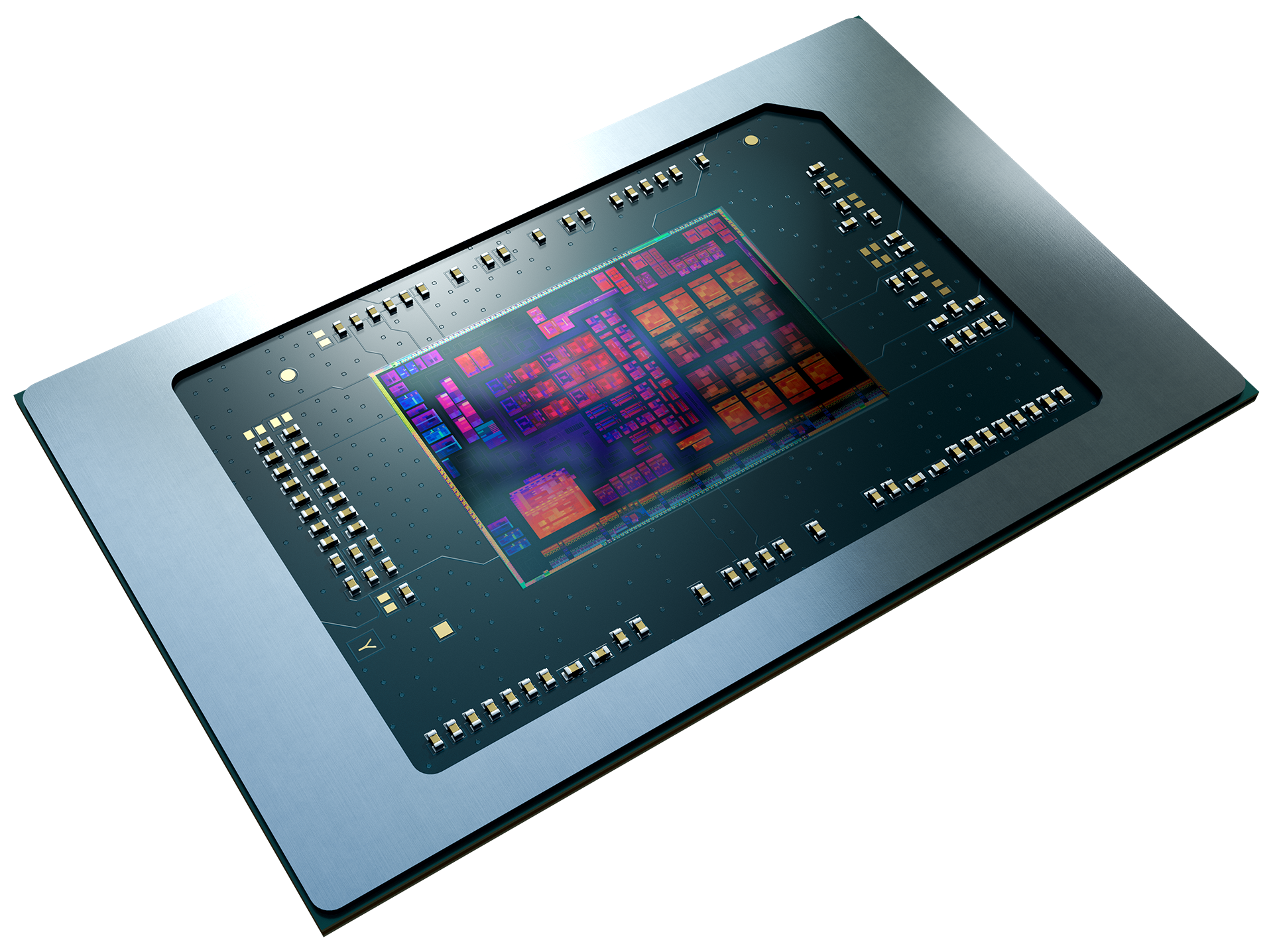
The AMD Ryzen 7 H 260 is a high-end notebook processor from the Hawk Point series with 8 cores and hyperthreading (SMT), which means it can process up to 16 threads simultaneously. At release, the CPU is only available in China and is technically practically identical to the older AMD Ryzen 7 8845HS or Ryzen 7 7840HS (slower AI engine).
The performance of the second-fastest model in the Hawk Point series should only be slightly behind the Ryzen 9 7940HS (+100 - 200 MHz clock, e.g. only 2% slower Turbo). As a result, the performance at 54W TDP should also be comparable to the AMD Ryzen 7 7745HX (also 8 Zen 4 cores, max 5.1 GHz, 55W, 32 MB L3) and thus clearly ahead of the old top model AMD Ryzen 9 6980HX resp. 6980HS (with lower TDP).
The chip integrates a modern RDNA 3-based graphics card (iGPU) called Radeon 780M with 12 CUs and up to 2.7GHz including AV1 video engine. Furthermore, a Xilinx FPGA-based XDNA AI accelerator is also integrated, which is now clocked higher. Hawk Point offers 2x USB 4 (40 Gbps), 20 PCIe 4.0 lanes and a dual-channel DDR5-5600 / LPDDR5x-7500 memory controller (with ECC support).
The Hawk Point series is a single chip (unlike the Dragon Range 7045HX series) and is manufactured at TSMC using the modern 4nm FinFET process.
Intel Core Ultra 7 265HX
► remove from comparisonThe Intel Core Ultra 7 265HX is a mobile high-end CPU for gaming notebooks based on the Arrow Lake architecture. It offers 20 cores consisting of 8 fast performance cores with up to 5.3 GHz and 12 of the 16 smaller efficiency cores with up to 4.6 GHz clock speed. The CPU can access 36 MB L2 cache and 36 MB L3 cache and is specified with a TDP of 55 Watts (160 Watts maximum Turbo).
The SoC integrates a small dedicated NPU called AI Boost with 13 TOPS (Int8) and optionally supports vPro Enterprise. The integrated memory controller supports up to 192 GB DDR5-6400 (dual channel, ECC optional). The integrated GPU (iGPU) is a small Intel Graphics graphics card with four Xe cores running at 300 - 1900 MHz.
Performance - High End
Thanks to the improved IPC of the cores (especially the efficiency cores), the CPU should be just before or at the level of the Raptor Lake Core i7-14700HX (8 + 12 cores, max 5.5 / 3.9 GHz). This makes the CPU ideal for demanding tasks such as high-end gaming and content creation.
Production - TSMC and Foveros
The Arrow Lake-HX chips are based on the desktop Arrow Lake-S chips and are composed of several chiplets. The CPU part is manufactured at TSMC in the modern N3B (3nm) process, the GPU also comes from TSMC in the N5P process. The SoC and I/O tile are manufactured in the TSMC N6 process. The base tile is manufactured by Intel in the 22nm process and carries the individual chiplets thanks to Fovero's 3D packaging.
| Model | Intel Core Ultra 5 245HX | AMD Ryzen 7 H 260 | Intel Core Ultra 7 265HX | ||||||||||||||||||||||||||||||||||||||||||||||||||||||||||||||||||||||||||||||||||||||||||||||||||||||||
| Codename | Arrow Lake-HX | Hawk Point-HS (Zen 4) | Arrow Lake-HX | ||||||||||||||||||||||||||||||||||||||||||||||||||||||||||||||||||||||||||||||||||||||||||||||||||||||||
| Series | Intel Arrow Lake | AMD Hawk Point (Zen 4/4c) | Intel Arrow Lake | ||||||||||||||||||||||||||||||||||||||||||||||||||||||||||||||||||||||||||||||||||||||||||||||||||||||||
| Series: Arrow Lake Arrow Lake-HX |
|
|
| ||||||||||||||||||||||||||||||||||||||||||||||||||||||||||||||||||||||||||||||||||||||||||||||||||||||||
| Clock | 2600 - 5100 MHz | 3800 - 5100 MHz | 2300 - 5300 MHz | ||||||||||||||||||||||||||||||||||||||||||||||||||||||||||||||||||||||||||||||||||||||||||||||||||||||||
| L2 Cache | 24 MB | 8 MB | 36 MB | ||||||||||||||||||||||||||||||||||||||||||||||||||||||||||||||||||||||||||||||||||||||||||||||||||||||||
| L3 Cache | 26 MB | 16 MB | 36 MB | ||||||||||||||||||||||||||||||||||||||||||||||||||||||||||||||||||||||||||||||||||||||||||||||||||||||||
| Cores / Threads | 14 / 14 6 x 5.1 GHz Intel Lion Cove P-core 8 x 4.5 GHz Intel Skymont E-core | 8 / 16 8 x 5.1 GHz AMD Zen 4 | 20 / 20 8 x 5.3 GHz Intel Lion Cove P-core 12 x 4.6 GHz Intel Skymont E-core | ||||||||||||||||||||||||||||||||||||||||||||||||||||||||||||||||||||||||||||||||||||||||||||||||||||||||
| TDP | 55 Watt | 45 Watt | 55 Watt | ||||||||||||||||||||||||||||||||||||||||||||||||||||||||||||||||||||||||||||||||||||||||||||||||||||||||
| TDP Turbo PL2 | 160 Watt | 160 Watt | |||||||||||||||||||||||||||||||||||||||||||||||||||||||||||||||||||||||||||||||||||||||||||||||||||||||||
| Technology | 3 nm | 4 nm | 3 nm | ||||||||||||||||||||||||||||||||||||||||||||||||||||||||||||||||||||||||||||||||||||||||||||||||||||||||
| iGPU | Intel Arc Graphics 3-core GPU (Arrow Lake) (300 - 1900 MHz) | AMD Radeon 780M ( - 2700 MHz) | Intel Graphics 4-Core iGPU (Arc) (300 - 1900 MHz) | ||||||||||||||||||||||||||||||||||||||||||||||||||||||||||||||||||||||||||||||||||||||||||||||||||||||||
| Architecture | x86 | x86 | x86 | ||||||||||||||||||||||||||||||||||||||||||||||||||||||||||||||||||||||||||||||||||||||||||||||||||||||||
| Announced | |||||||||||||||||||||||||||||||||||||||||||||||||||||||||||||||||||||||||||||||||||||||||||||||||||||||||||
| Manufacturer | www.intel.com | www.amd.com | www.intel.com | ||||||||||||||||||||||||||||||||||||||||||||||||||||||||||||||||||||||||||||||||||||||||||||||||||||||||
| L1 Cache | 512 KB | ||||||||||||||||||||||||||||||||||||||||||||||||||||||||||||||||||||||||||||||||||||||||||||||||||||||||||
| Die Size | 178 mm2 | ||||||||||||||||||||||||||||||||||||||||||||||||||||||||||||||||||||||||||||||||||||||||||||||||||||||||||
| max. Temp. | 100 °C | ||||||||||||||||||||||||||||||||||||||||||||||||||||||||||||||||||||||||||||||||||||||||||||||||||||||||||
| Socket | FP7/FP7r2/FP8 | ||||||||||||||||||||||||||||||||||||||||||||||||||||||||||||||||||||||||||||||||||||||||||||||||||||||||||
| Features | DDR5-5600/LPDDR5x-7500 RAM, PCIe 4, Ryzen AI, MMX, SSE, SSE2, SSE3, SSSE3, SSE4A, SSE4.1, SSE4.2, AVX, AVX2, AVX-512, BMI2, ABM, FMA, ADX, SMEP, SMAP, SMT, CPB, AES-NI, RDRAND, RDSEED, SHA, SME |

Benchmarks

Average Benchmarks Intel Core Ultra 7 265HX → 0% n=0
* Smaller numbers mean a higher performance
1 This benchmark is not used for the average calculation