US next-gen BAT laser system aims for a 10x efficiency boost for EUV chip production
Lawrence Livermore National Laboratory (LLNL) is developing a petawatt-class laser system that could significantly boost the efficiency of EUV lithography equipment used in chip manufacturing. Known as the Big Aperture Thulium (BAT) laser, this technology aims to achieve roughly ten times the efficiency of the CO2 lasers currently dominating the industry.
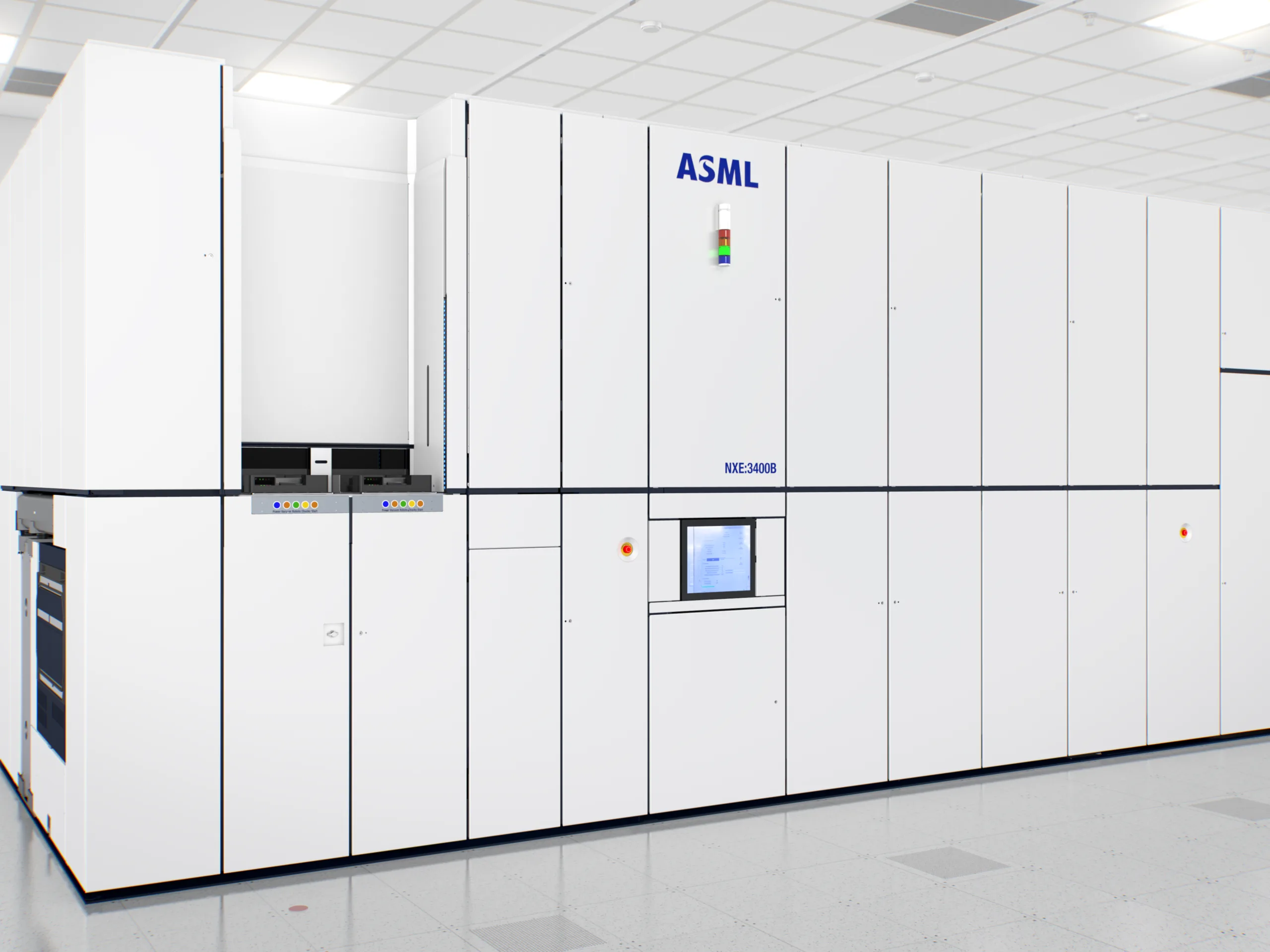
This initiative falls under a new four-year, $12 million project at the Extreme Lithography & Materials Innovation Center (ELMIC), backed by the Department of Energy’s Microelectronics Science Research Centers program. It’s a team effort, with input from SLAC National Accelerator Laboratory, ASML San Diego, and the Advanced Research Center for Nanolithography (ARCNL).
The BAT laser employs thulium-doped yttrium lithium fluoride as its gain medium. It runs at a wavelength of about 2 microns—quite a departure from today’s powerful lasers, which typically operate around 1 micron or 10 microns. This novel wavelength could yield a more efficient plasma-to-EUV conversion when it hits tin droplets in the lithography process.
Currently, EUV lithography systems consume a lot of power—up to 1,400 kilowatts for high-NA EUV tools. Most of this energy is used to heat tin droplets to a blazing 500,000°C to create plasma that emits the needed 13.5-nanometer light. Using diode-pumped solid-state technology, the BAT laser might improve energy efficiency and heat management compared to today’s CO2 lasers.
Laser physicist Brendan Reagan and plasma physicist Jackson Williams, who are co-principal investigators, are spearheading the project. Their research builds on five years of plasma simulations and early proof-of-concept tests that have already caught the attention of the EUV lithography community.
All the testing will happen at LLNL’s Jupiter Laser Facility, which just finished a major four-year upgrade. This facility is part of LaserNetUS, a network of high-power laser labs across North America funded by the Department of Energy’s Office of Science.
While the BAT laser technology could speed up chip production and lower power usage, rolling it out in the semiconductor industry will be a big challenge. It would require significant changes to existing infrastructure, and that kind of transition isn’t likely to happen overnight. After all, today’s EUV systems took decades to go from concept to full production.
Source(s)
LLNL (in English)
