Nano-scale perovskite LEDs shatter size and efficiency records for next-gen displays
Scientists from Zhejiang University and the University of Cambridge have unveiled nano-scale perovskite LEDs that measure just 90 nanometers across. These LEDs shatter the previous record for LED miniaturization while still delivering high efficiency.
Unlike traditional micro-LEDs based on III-V semiconductors, which tend to lose a lot of efficiency below 10 micrometers, these perovskite LEDs maintain about 20 percent external quantum efficiency across a wide range of pixel sizes (from 650 down to 3.5 microns). This feat potentially revolutionizes high-resolution display technology, especially for advanced AR/VR systems.
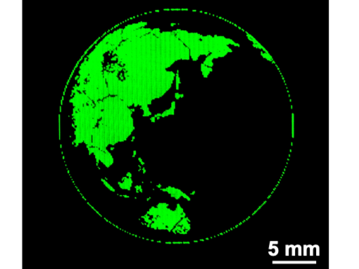
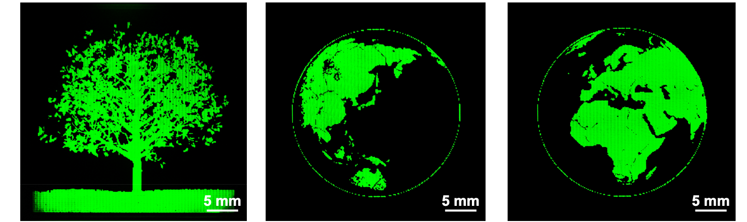
These new nano-PeLEDs pack an astounding 127,000 pixels per inch (PPI)—the highest pixel density reported in any LED array so far. Standard LED technology usually suffers a steep efficiency drop when shrunk to the smaller dimensions needed for next-generation displays.
Highlighting the significance of this achievement, Professor Zhao Baodan from Zhejiang University remarked:
Currently, the most advanced technology for display applications is micro-LEDs. They are the best light source for augmented reality (AR) and virtual reality (VR) applications. However, the efficiency of micro-LEDs drops rapidly when the pixel sizes are smaller than 10 micrometers, which are the desirable pixel sizes for high-end AR/VR applications with ultra-high resolutions.
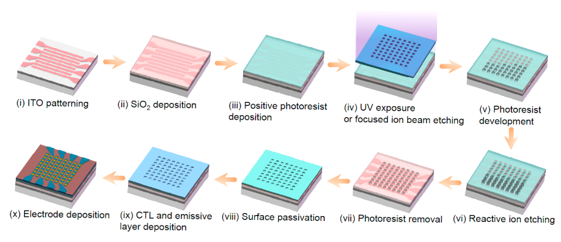
The team devised an innovative fabrication technique to overcome the usual challenges of working with perovskite materials. PhD student Lian Yaxiao, lead author of the paper, noted, “Conventional photolithographic processes are not suitable for the direct patterning of the perovskite layers—it would damage the perovskite materials so that we have to pattern the other functional layers instead.”
Their method relies on a localized contact fabrication setup that uses lithographically created windows in an insulating layer. This design keeps active pixels clear of electrode edges, reducing non-radiative losses that normally undermine LED efficiency.
Beyond the lab, the researchers have already taken steps toward practical applications. Teaming up with Hangzhou-based LinkZill, a company specializing in thin-film transistor (TFT) technology, they developed a prototype active-matrix micro-PeLED display driven by a TFT backplane. This display, capable of showcasing detailed images and video clips, brings these cutting-edge LEDs one step closer to commercial use.
Source(s)
ZJU (in English)
