Intel and LEGO team up to help visualize what makes Lakefield so special
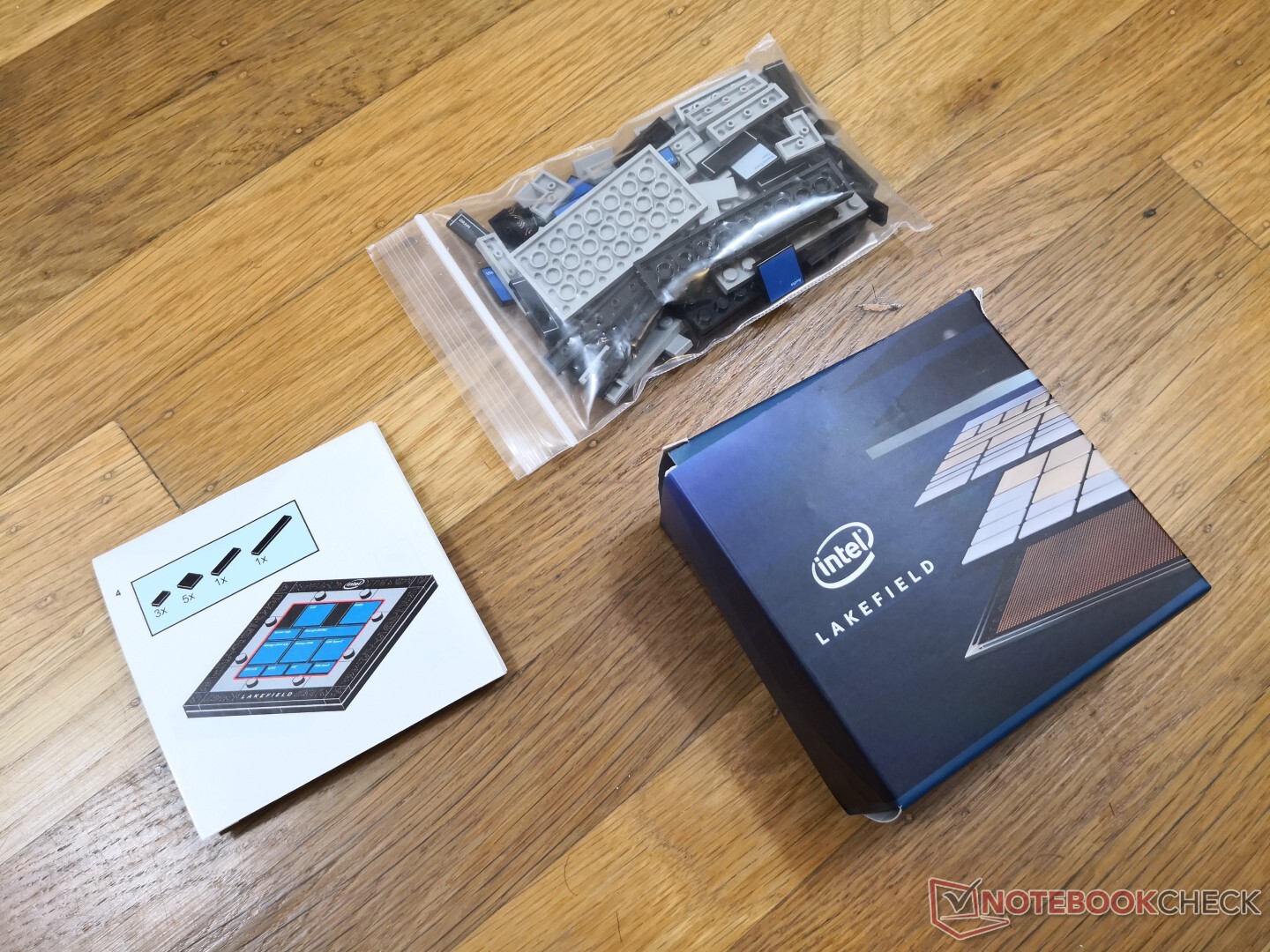
To celebrate the launch of Lakefield, Intel sent us an 89-piece Lego set showing off the innards of the hybrid processor. The full details of the groundbreaking 3D micro-architecture can be found via press release here. It may not be 7 nm, but it's a special series nonetheless with significant performance and power-efficiency advantages over the aging Amber Lake-Y series. The first laptops powered by Lakefield are expected to launch in the coming months.
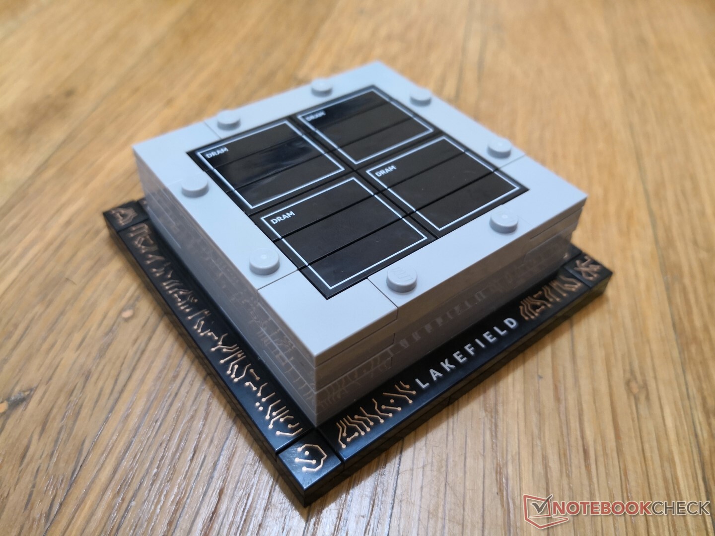
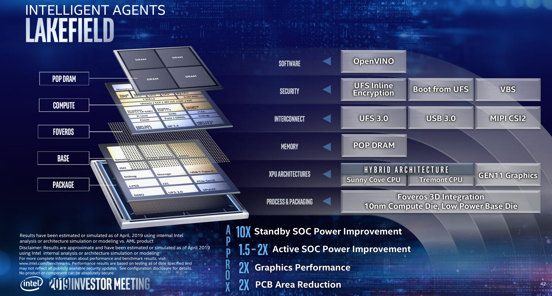
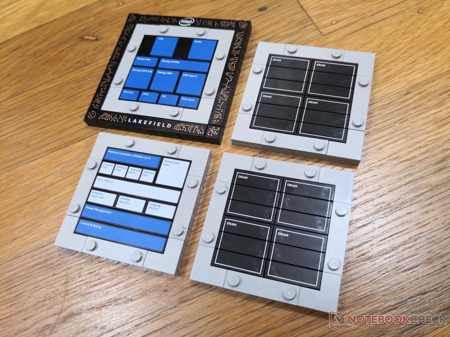
The Lego set is separated into four chiplets to represent the different layers of a Lakefield processor: the package base, the compute layer, and the two package-on-package (POP) DRAM layers.
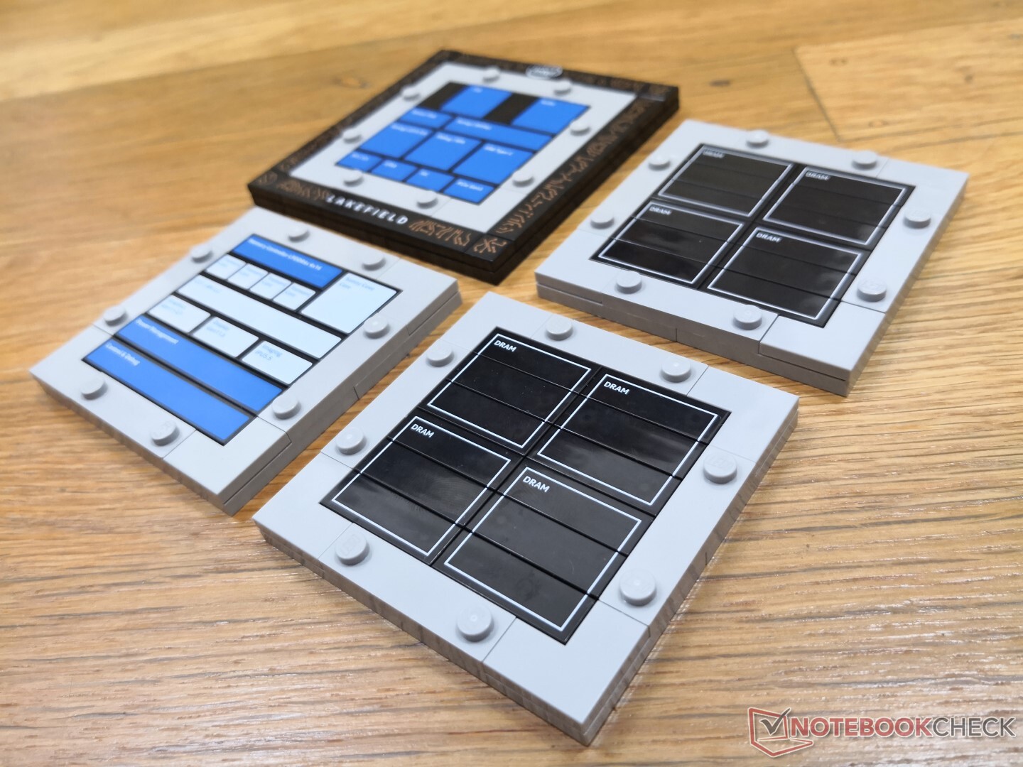
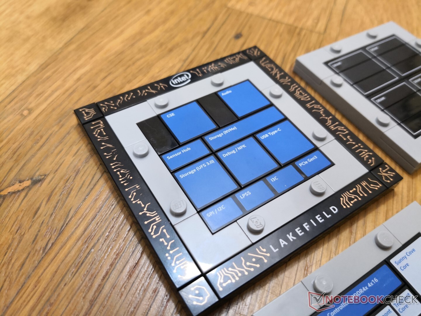
The package base lies on the very bottom and it's responsible for I/O processing including USB Type-C, NVMe storage, and others.
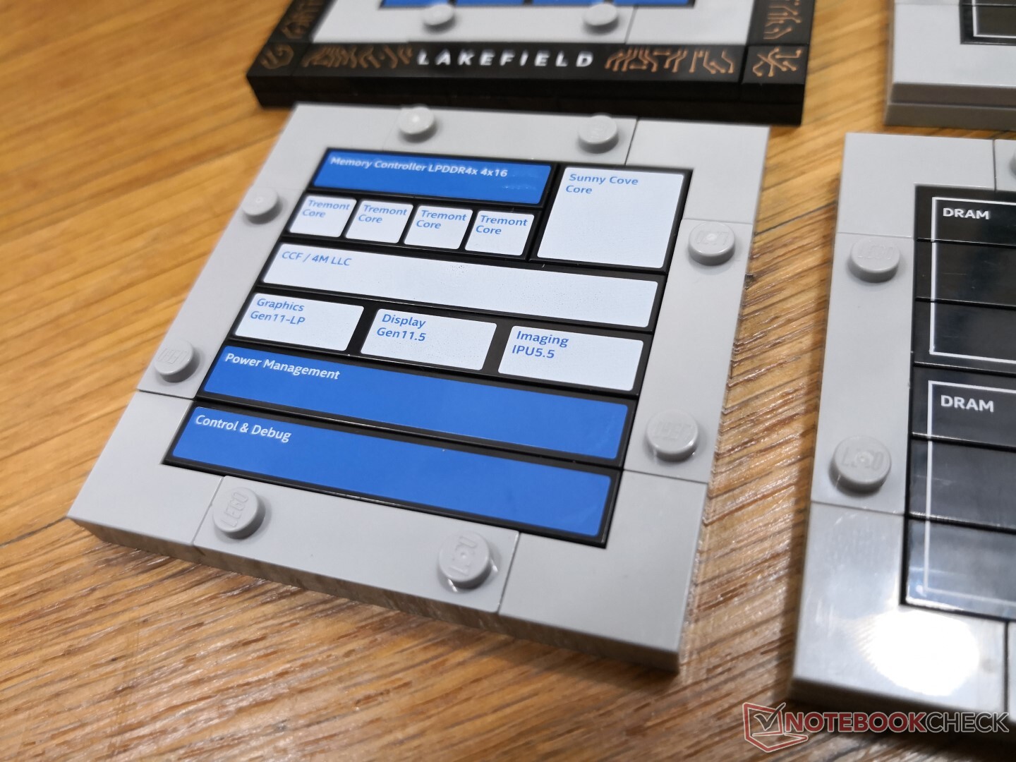
On top of the package die is the compute layer which houses the four low-power Tremont Atom cores and the single, more powerful 10 nm Sunny Cove core derived from Ice Lake. The integrated UHD Graphics sits here as well.
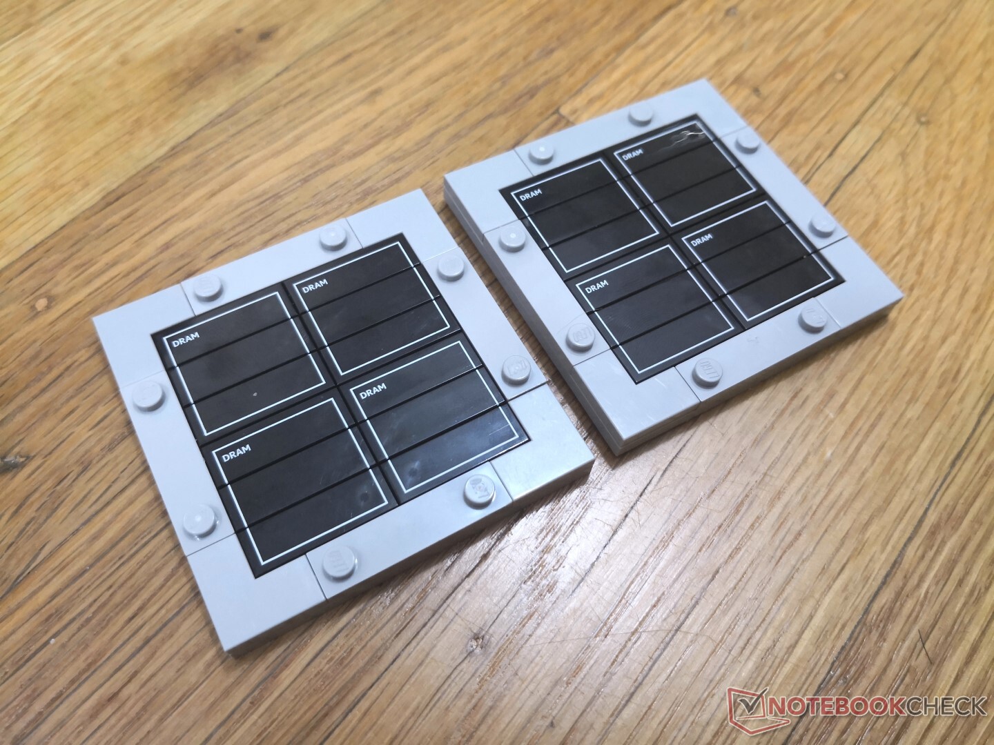
Finally, sitting on top of the compute layer are the two POP DRAM layers. All four chiplets are stacked together using a technique that Intel markets as Foveros.
The resulting SoC measures only 12 x 12 x 1 mm to both reduce the space needed on a motherboard and allow for smaller laptop designs.
Explaining advanced micro-architectures with plastic building blocks can only get you so far, but it's definitely a fun and unique approach nonetheless. Hopefully Intel will do the same when Xe graphics cards become available!