Chinese company Prinano delivers first domestic nanoimprint lithography tool
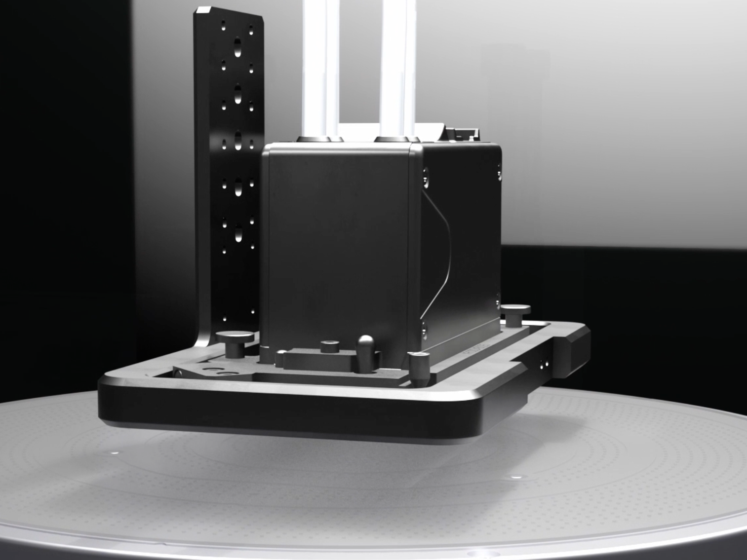
Chinese equipment maker Prinano has delivered its first self-developed PL-SR step-and-repeat nanoimprint lithography system to a domestic customer focused on specialty processes. It is positioned for actual chip production after customer-side testing and makes Prinano only the second company, after Canon, to place a nanoimprint tool with a client.
According to the provided materials, the PL-SR supports line widths below ten nanometers. Canon's FPA-1200NZ2C achieves around fourteen nanometers line width. It is promoted as enabling five-nanometer-class chips, but the documents caution that Prinano's result does not mean the PL-SR can manufacture advanced logic at a five-nanometer node.
The appeal of nanoimprint here is straightforward: it avoids the extreme ultraviolet light sources used in commercial EUV lithography, curbing energy use and equipment cost. The trade-off is throughput and flexibility. Nanoimprint remains slower than conventional optical lithography and is a poor fit for complex logic processes with intricate, advanced patterns.
Prinano's machine patterns wafers by pressing a rigid quartz mold, engraved with nanoscale circuitry, into a thin, inkjet-deposited resist layer. The system's inkjet module dynamically meters droplet volume to keep the residual layer thin (under ten nanometers with less than two nanometer variation), then cures the pattern for subsequent etch. The tool handles 300 mm wafers, aligns the mold and wafer to fine tolerances, and imprints each field sequentially with stitching to cover the full wafer. It also supports uniform template joins from 20 mm x 20 mm up to 300 mm x 300 mm.
A proprietary template-profile control mechanism aims to compensate for mold-to-wafer curvature mismatches, enabling transfer of features with aspect ratios above seven-to-one while limiting distortion, an important practical concern for yield and device variability. After imprinting, the resist serves as the mask for etching the final structures.
Initial validation targets applications with regular, repetitive patterns: NAND Flash, silicon-based microdisplays, silicon photonics, and advanced packaging. These domains benefit from the technology's fine pitch and field-by-field stitching without demanding the pattern diversity typical of CPUs and GPUs. The material also frames domestic nanoimprint as a way for Chinese memory makers to trim dependence on foreign tools and compete more effectively against established suppliers.
Source(s)
ICsmart (in Chinese)
