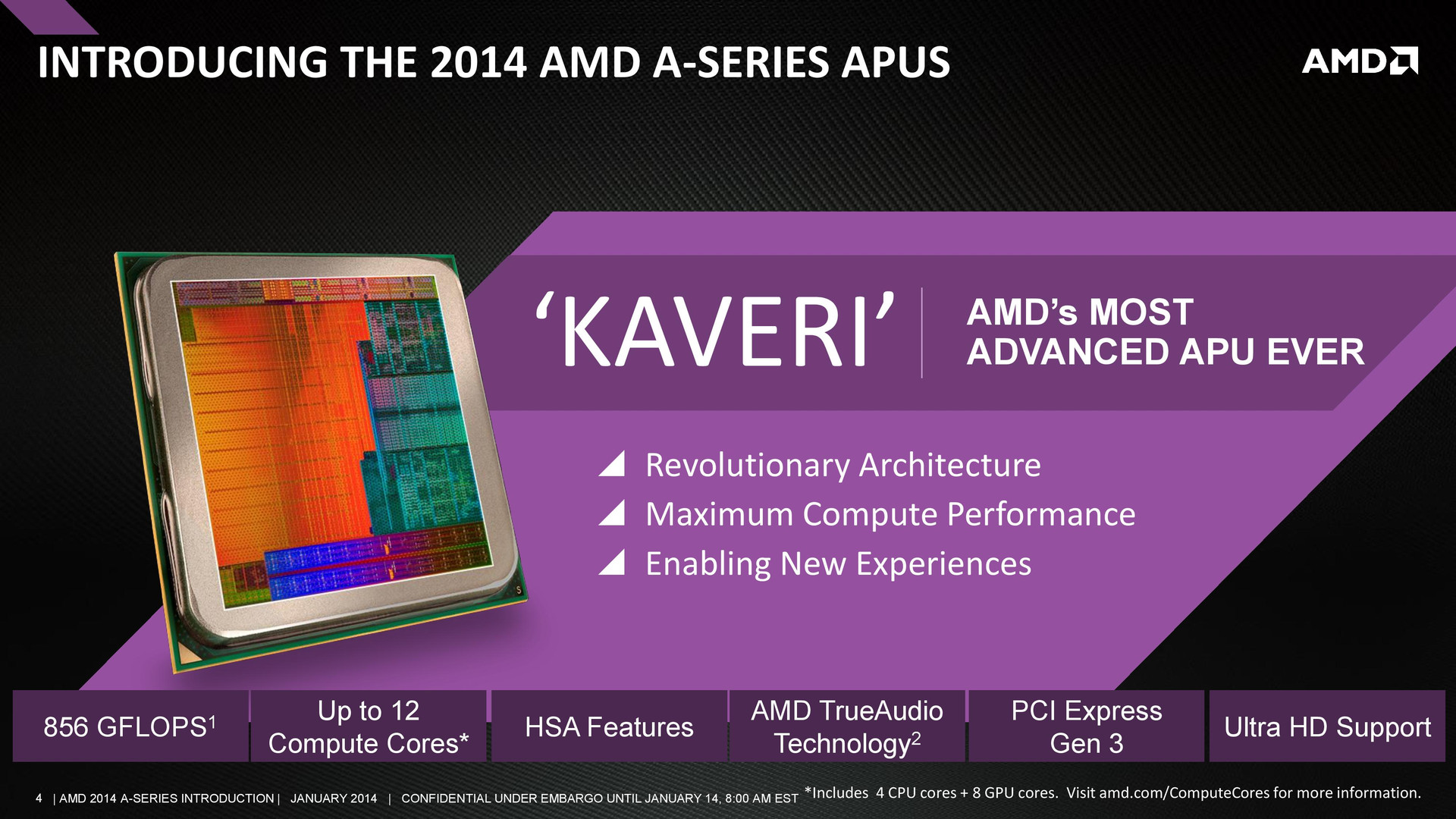
AMD reveals Kaveri APU series
Welcome to the revolution. AMD hypes its latest APU generation, codenamed "Kaveri", with powerful promises to keep. Even if today's launch revolves around desktop models only, we are still eager to take a quick look at some of the changes and new features that the new chips will bring.
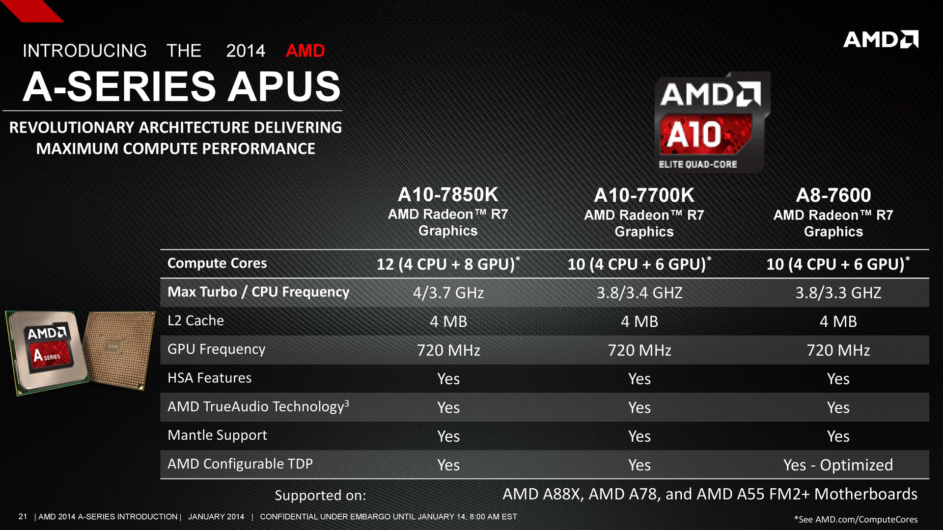
We begin with the first two announced models: the A10-7850K and A10-7700K. A third model, the A8-7600, is expected to follow later in the first quarter. The official technical specifications for these models are as follows:
| A10-7850K | A10-7700K | A8-7600 | |
| Cores (Module) | 4 (2) | 4 (2) | 4 (2) |
| CPU Speed | 3.7 GHz | 3.4 GHz | 3.1 GHz / 3.3 GHz |
| CPU Turbo | 4.0 GHz | 3.8 GHz | 3.3 GHz / 3.8 GHz |
| GPU Cores | 8 (512 Shaders) | 6 (384 Shaders) | 6 (384 Shaders) |
| GPU Speed | 720 MHz | 720 MHz | 720 MHz |
| TDP | 95 W | 65 W | 45 W / 65 W |
| MSRP | 173 $ | 152 $ | 119 $ |
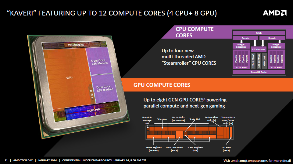
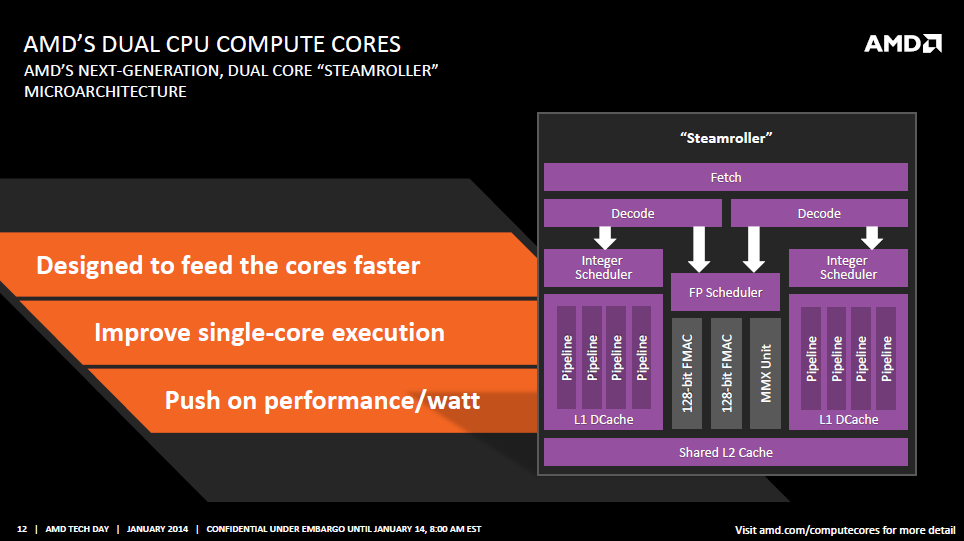
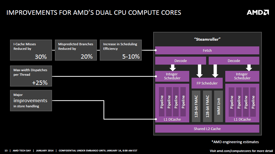
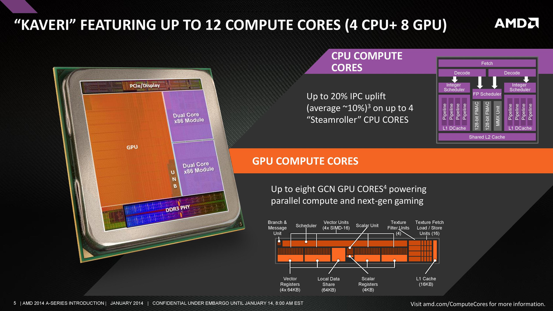
Like its predecessors Trinity and Richland, Kaveri builds upon the Bulldozer design. A maximum of two modules are available with two cores, though AMD mentions four compute cores in its PR. The new architecture is expected to outperform Steamroller and Piledriver (Trinity/ Richland) by about 10 percent in terms of performance-per-watt due to improved branch prediction, additional decoders and a higher L1 cache.
Despite these optimizations, final CPU performance is only barely above its predecessor; The base and Turbo clock rates of Kaveri are slightly lower than Richland.
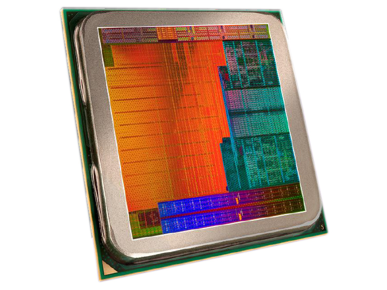
The reason for this lies in the new 28 nm SHP process at GlobalFoundries. This process was developed specifically for Kaveri to satisfy the different demands of the CPU and GPU portions of the APU. By allowing both very high clock rates in one area and a denser packing in another, AMD claims to have been able to fit 2.41 billion transistors in an area of just 245 mm2. In contrast, a typical 32 nm Richland APU was of a very similar size made up of "only" about 1.3 billion transistors.
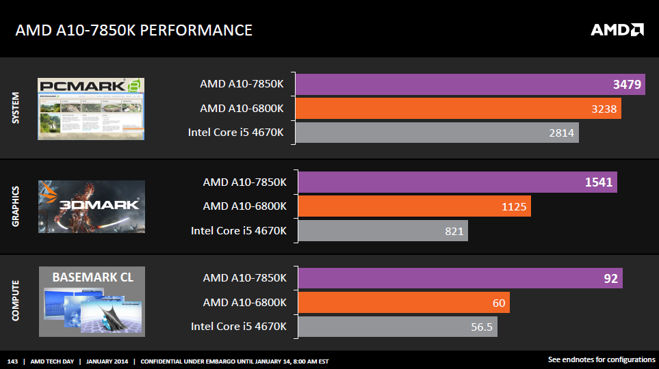
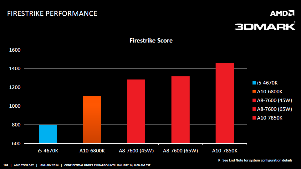
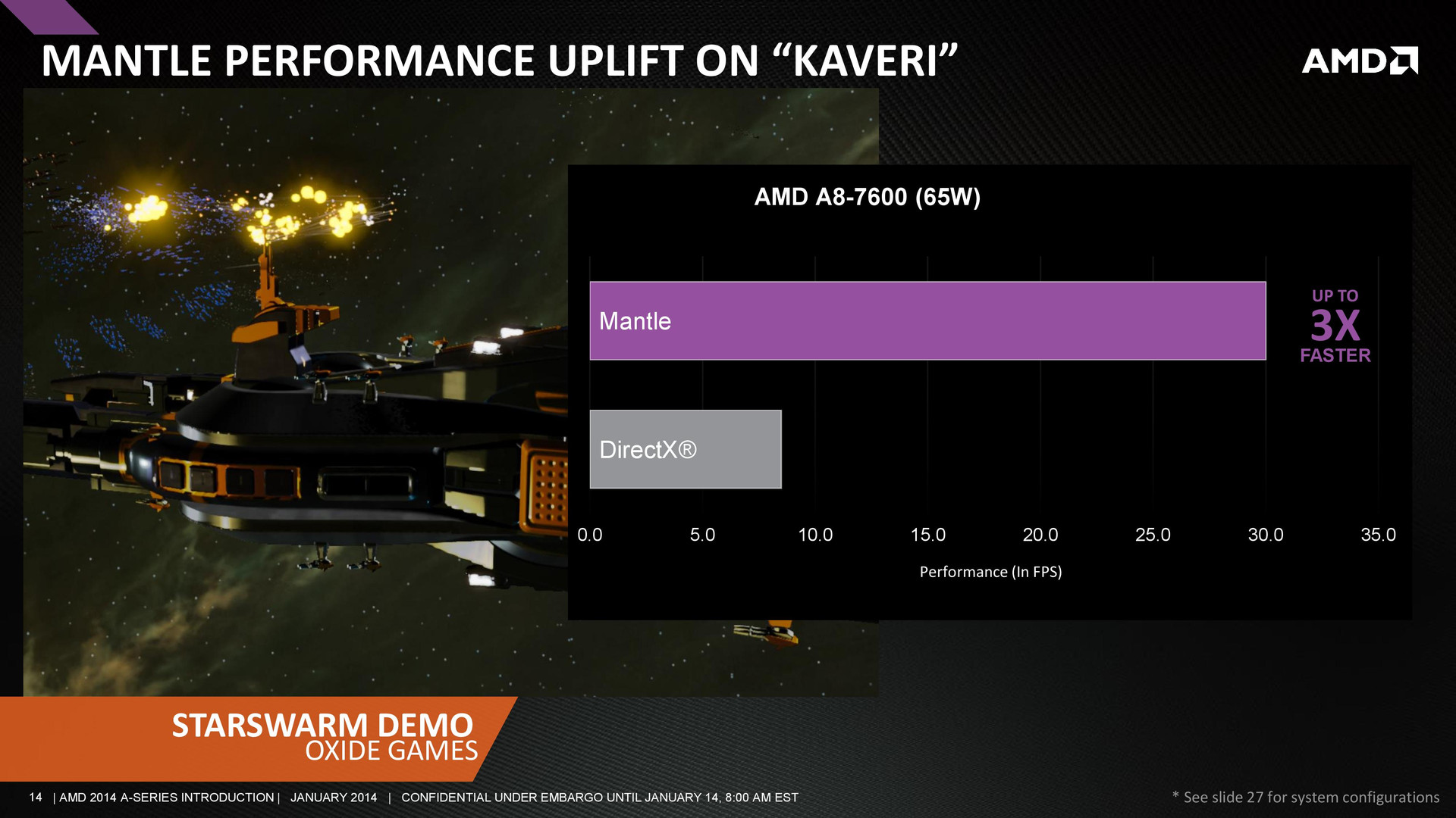
The increased transistor budget was heavily invested in the integrated GPU. Kaveri has upped the number of VLIW4 ALUs from 384 shaders in Trinity/ Richland to 512 shaders and 8 Compute Units, all based on the GCN architecture with cues from the Radeon R9 290X GPU. In addition to the DirectX 11.2 and Mantle API feature sets, raw GPU performance has increased noticeably. The 45 W A8-7600, for example, returned results that were about 30 percent higher than the previous A10-6800K leader in 3DMark Fire Strike, according to AMD.
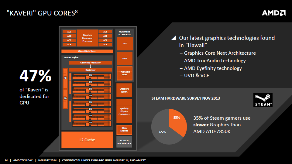
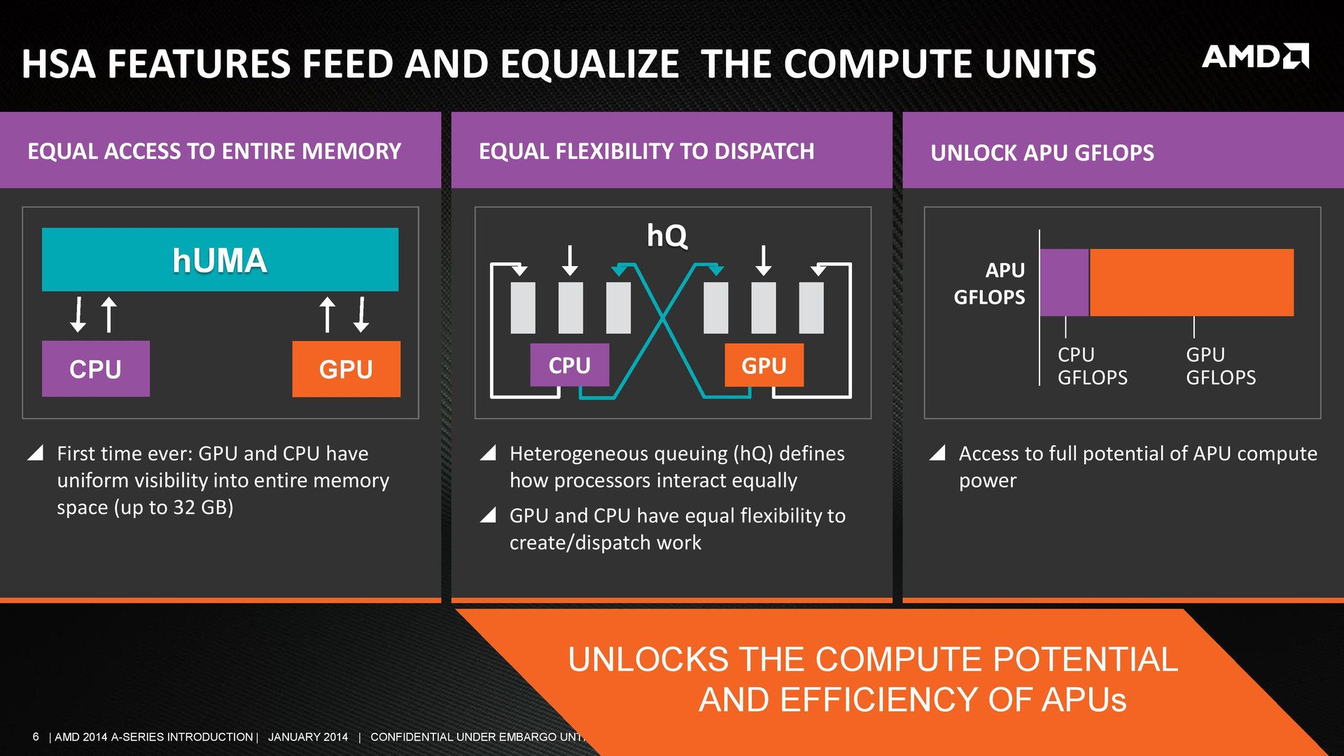
Another major feature of Kaveri is the HSA (Heterogenous System Architecture) concept. Various monitoring tools will help ensure that the entire APU and GPU can be used as efficiently as possible for general calculations. Meanwhile, HUMA (Heterogenous Uniform Memory Access) will allow for data that can be more easily shared and addressed between the CPU and GPU for reduced latency and power consumption. A similar technology can be found in the XBox One and Playstation 4 consoles which, perhaps unsurprisingly, are powered by AMD APUs.
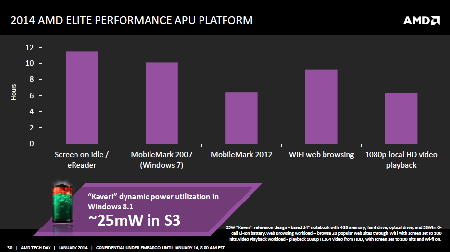
Beyond the Kaveri reveal, we are particularly excited about the eventual notebook APU models. Though AMD has remained mum, users should expect Kaveri to appear in the low-power segment for notebooks. DDR3-2400 support is not expected, but performance gains are expected followed by increased battery life in S3 mode. Depending on Intel's roadmap, Kaveri may very well be face-to-face with Broadwell soon after its launch instead of the current Haswell generation.


Source(s)
Notebookcheck.com
