TSMC releases more details regarding the upcoming 3 nm node
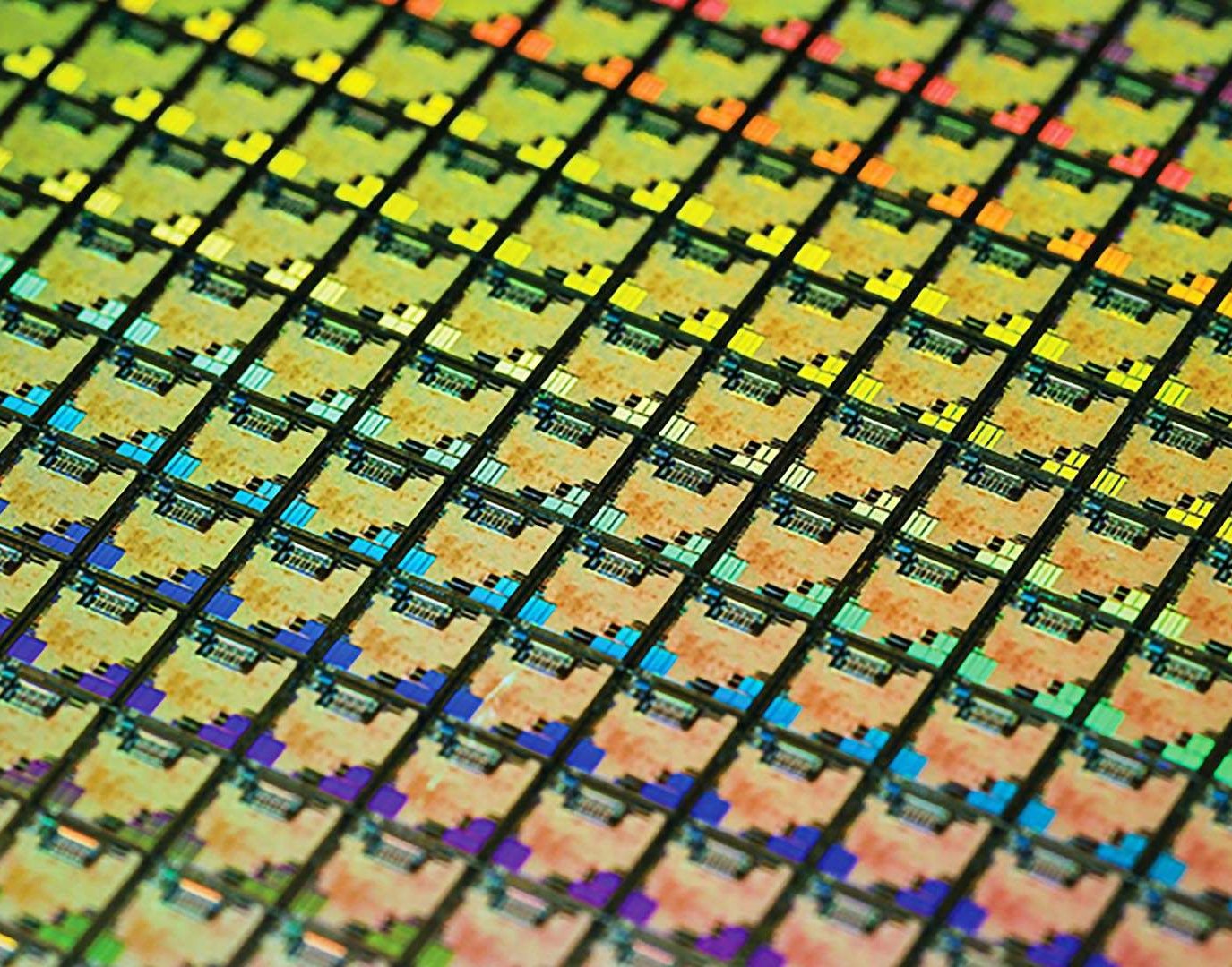
A few days ago TSMC was celebrating the billionth chip produced on the 7 nm nodes, but the Taiwanese company is now looking towards the near future as it just unveiled new details for the 5 nm and 3 nm nodes.
As far as the 5 nm node (N5) is concerned, TSMC stated that it is using the deep-ultraviolet (DUV) and extreme-ultraviolet (EUV) processes, and the first 5 nm chips to be released later this year should include Apple’s next gen A14 Bionic SoCs. TSMC also reports that N5 already has better yields at current production times compared to previous N7 and N10 nodes, and projected defect densities are expected to improve well beyond historic trends.
Between N5 and N3, TSMC plans to introduce two additional nodes. First is the N5P, which is a slightly improved version of the N5, expected to increase performance by 5% and reduce power requirements by 10% some time in 2021. The other process will come in the form of the N4 node that will refine the existing EUV layers reducing the number of required masks, with risk production planned for late 2021 and volume production scheduled some time in 2022.
N3 is planned for H2 2022, but it looks like TSMC is not going to try to implement the gate-all-around (GAAFET) transistor structure. Apparently, this type of transistors is still too complicated to implement, requiring too many changes with the production facilities. Intel tried to implement the GAAFET transistors for its 7 nm nodes, but had to give up and postpone the launch to 2022, while Samsung appears to be the only one still developing the GAAFET structures for its upcoming 3 nm nodes. Instead of the GAAFET transistors, TSMC will be using FinFET tech with “innovative features.” However, despite using a refreshed version of the older FinFET tech, TSMC estimates that its N3 node would be superior in terms of density when compared to Samsung’s 3 nm GAAFET nodes.
Improvements for the N3 node over the N5 include 25-30% reduced power requirements, 10-15% increased performance, and 1.7x increase in transistor density leading to a 42% reduction in size (0.58 logic area).
