Samsung introduces its "industry-first" EUV-made DDR4 DRAM
EUV is a form of lithography normally reserved for processors and other related chipsets. It is capable of the high-precision, highly-focused pattern-generation necessary to create the 7-nanometer (nm) architectures found in high-end SoCs - not to mention their even smaller next generations. However, Samsung has also recently been applying this process to the production of DRAM chips, for similar reasons.
Indeed, the OEM asserts that the use of EUV in this area results in improved performance, greater yields and reduced development periods. In other words, it will allow the company to produce increased volumes of high-end memory in refined time-frames compared to older methods.
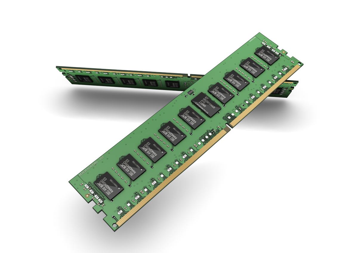
The newer technique has come to fruition in the form of the 10nm-class D1x DDR4 memory intended for buyers in the IT industry. Its successful development is to be followed by the mass-production of fourth-generation 10nm-class D1a Samsung DRAM.
This memory is DDR5 or LPDDR5, and will be joined in the company's higher-end 14nm-class memory chips in being made using an EUV process in the immediate future. Currently, Samsung projects that volume production of the D1a-based chips will begin in 2021.
Source(s)