Intel details new process innovations and node names, Alder Lake 10 nm Enhanced SuperFin is now Intel 7; Intel 20A is the 2 nm process for 2024
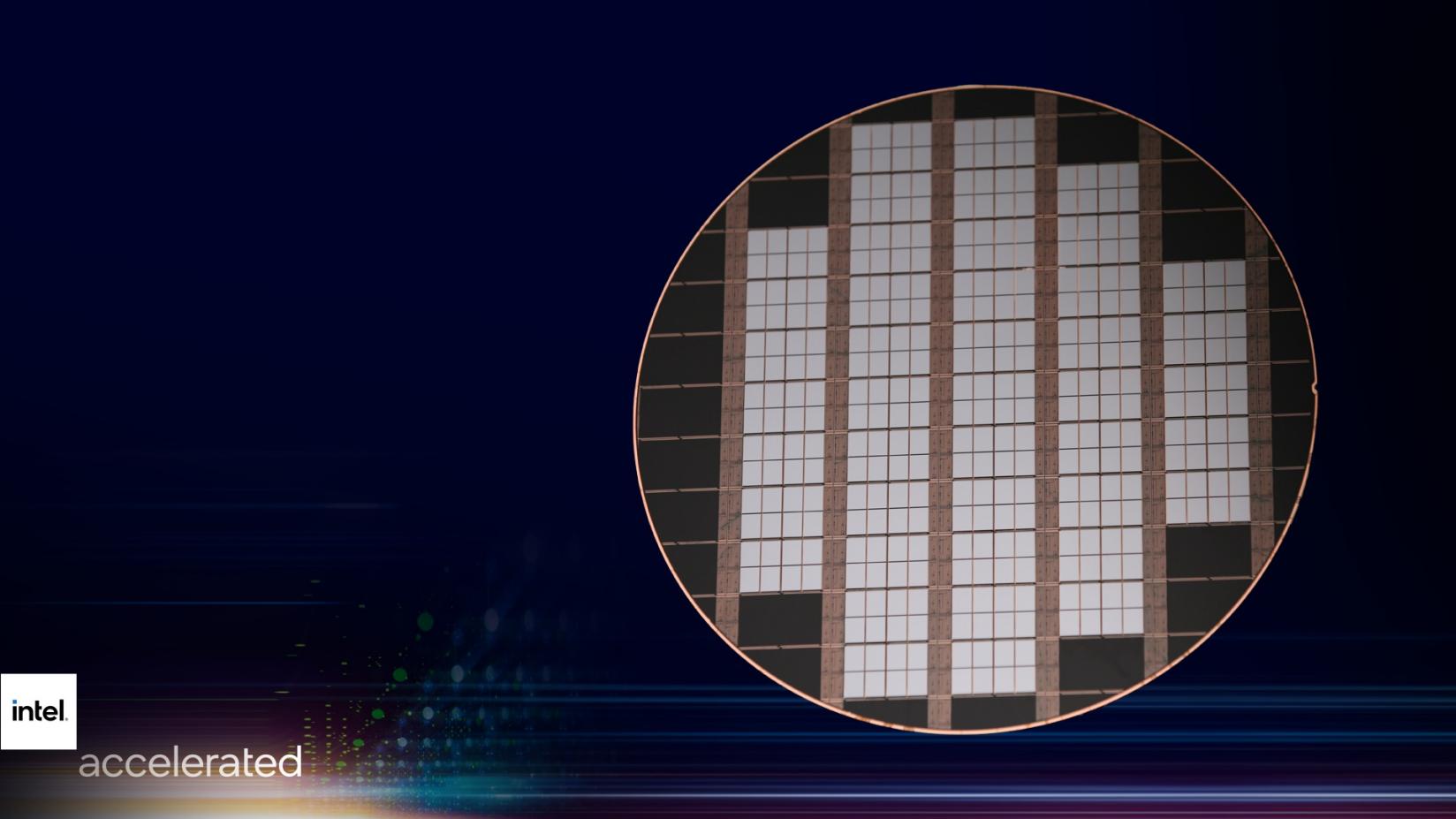
Intel has detailed a slew of process and packaging innovations as part of its integrated device manufacturing (IDM) 2.0 strategy during its Intel Accelerated webcast today. These innovations give us a picture of Intel's process roadmap through 2025 and beyond.
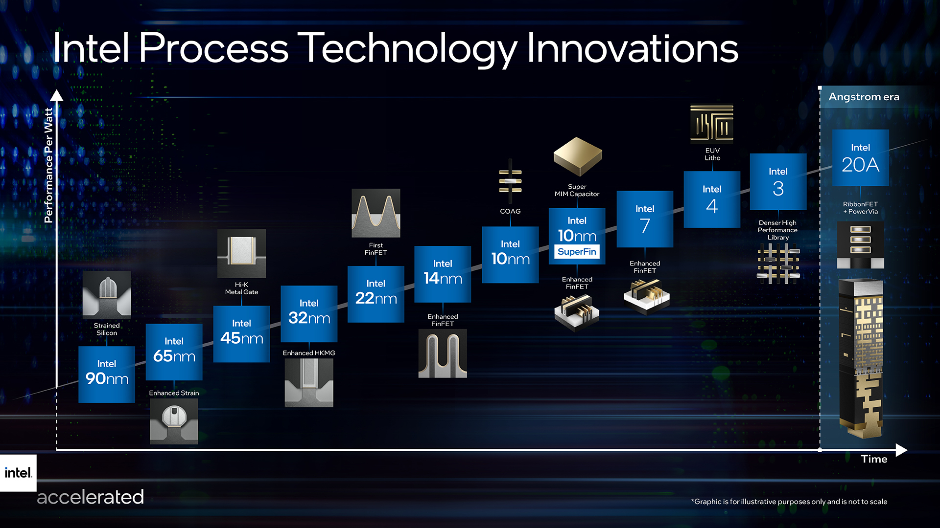
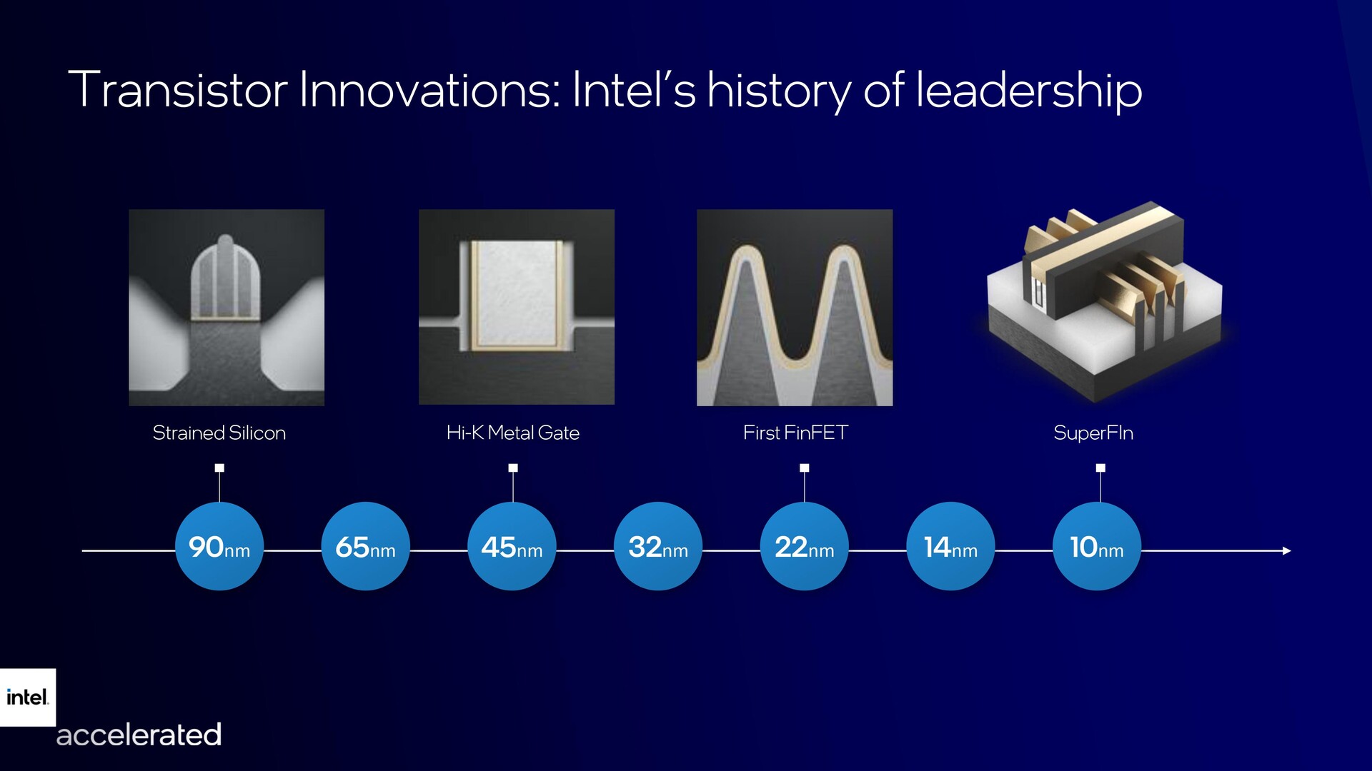
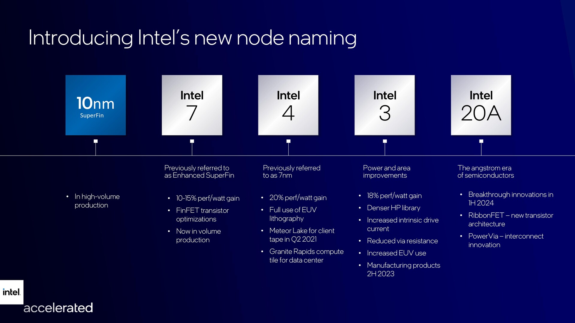
Intel feels the numbers denoted to indicate a process node are "just numbers" and that there is an inherent inconsistency in the current naming scheme. Therefore, the company will no longer indicate the process node in terms of nanometers but will use a new numbering scheme as follows:
Intel 7: This is the new name for 10 nm Enhanced SuperFin process and will feature in Alder Lake (client, 2021) and Sapphire Rapids (datacenter, Q1 2022) processor families. Intel 7 is slated to offer a 10% to 15% performance increase over the current 10 nm SuperFin process.
Intel 4: This is Intel's actual 7 nm part that uses extreme ultraviolet (EUV) lithography with an estimated 20% increase in performance-per-watt. Intel 4 will feature in products such as Meteor Lake (client) and Granite Rapids (datacenter) for production in 2H 2022 and shipping in 2023. The ultra-short EUV wavelength enables Intel to offer features such as 192 execution units (EUs) in Meteor Lake's iGPU and significantly enhanced core counts (up to 120?) for a dual-die Granite Rapids processor.
Intel 3: Intel 3 will see the final, maximum leverage of FinFET optimizations. FinFET first debuted with 22 nm Ivy Bridge processors back in 2011 and has since come a long way. Intel 3 uses increased EUV for an approximately 18% performance-per-watt increase over Intel 4 along with additional area improvements. Intel 3 will begin manufacturing in 2H 2023.
Intel 20A: With Intel 20A, we are officially entering into the Angstrom era (10 Angstrom = 1 nm). Intel 20A will see the introduction of a new transistor architecture named RibbonFET for faster transistor switching while achieving the same drive current in a smaller footprint. Debuting alongside RibbonFET is PowerVia, the company's first implementation of a backside power delivery mechanism that negates the need for power routing on the front of the wafer.
Intel 20A will ramp up in 2024 with Qualcomm expected to be one of the partners that will leverage this process node.
Intel 18A and beyond: Intel said that Intel 18A is already in development for early 2025. Intel 18A will use further refinements in RibbonFET and will be among the first to receive and deploy high numerical aperture (NA) EUV lithography in collaboration with lithography giant ASML.
Apart from the aforementioned process improvement, Intel also detailed its packaging roadmap. Intel Foundry Services (IFS) is also getting its first customer with Amazon AWS.
EMIB: EMIB packaging was first shown off during the launch of Kaby Lake-G processors back in 2017. Intel will continue to invest in EMIB with Sapphire Rapids slated to be the first Xeon family to implement it. Intel said this will be the first dual-reticle sized device in the industry that compares with a monolithic design. The next generation EMIB will move from a 55 micron bump pitch to 45 microns.
Foveros: Foveros is Intel's 3D packaging solution that first debuted with Lakefield processors. The second generation of Foveros will be seen in Meteor Lake in 2022 and will feature a bump pitch of 36 microns, tile-spanning multiple technology nodes, and a TDP between 5 W and 125 W.
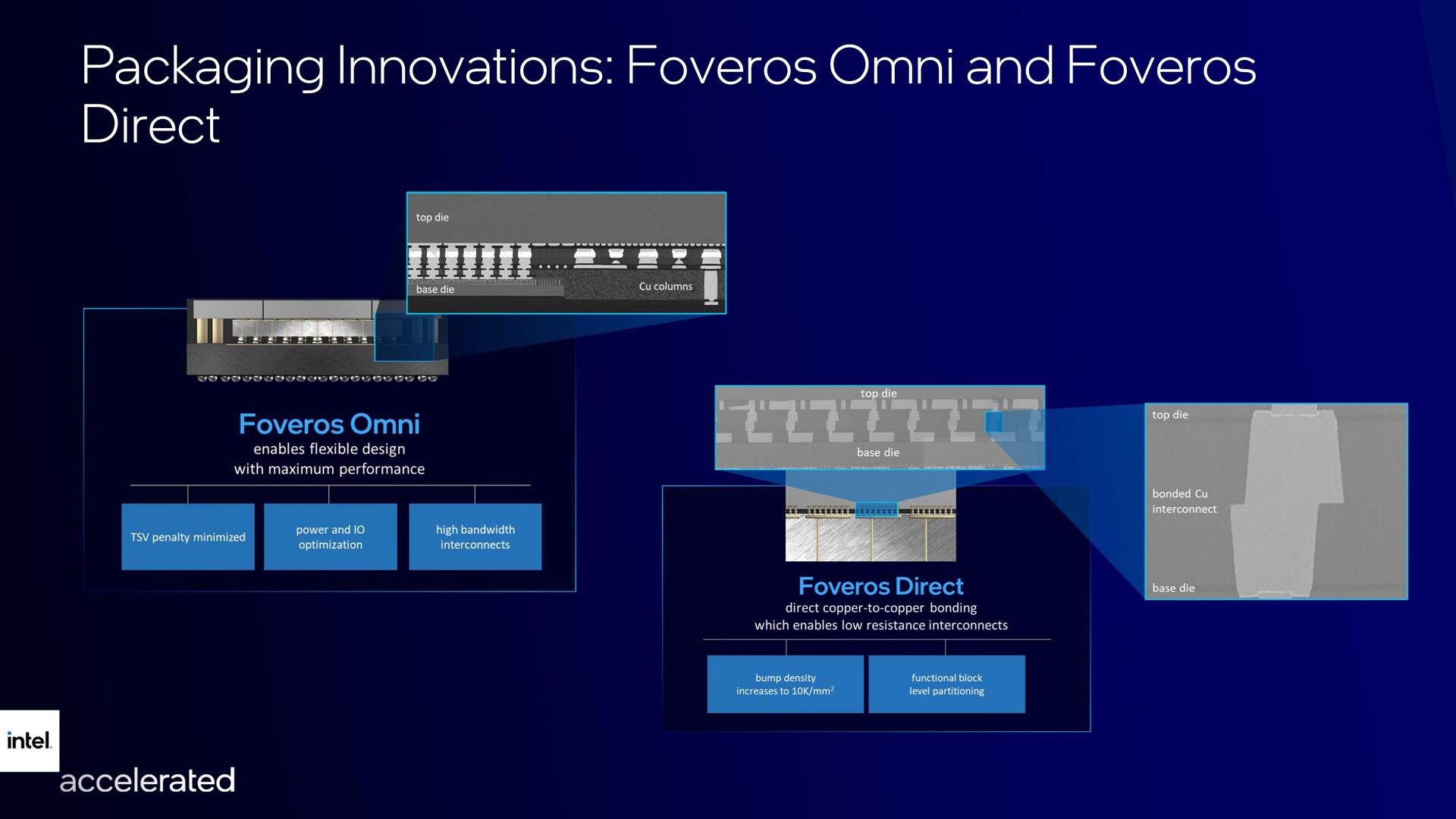
Foveros Omni: Foveros Omni allows for even further heterogeneity in top and base tiles of the package across different nodes. It is expected to begin volume manufacturing in 2023.
Foveros Direct: Foveros Direct will compliment Foveros Omni in 2023, enabling sub-10 nm bump pitches for even higher interconnect density in 3D stacking. Foveros Direct will use direct copper-to-copper bonding for low-resistance interconnects and will blur the line between the package and the wafer.
The company said that more information on process and packaging will be available during the Intel InnovatiON event to be held in San Francisco on October 27-28, 2021.


Source(s)
Intel Accelerated Webcast
