IBM presents the world's first 2 nm chips

IBM is proving once again that it is still one of the prominent companies pushing for cutting edge technology advancements with the introduction of the world’s first 2 nm semiconductors. The breakthrough is years ahead of similar endeavors coming from TSMC and Samsung that expect to bring 2 nm nodes online by 2023. IBM’s 2 nm production process is said to achieve 45 percent increased performance and up to 75 percent lower energy use over the most advanced 7 nm nodes from TSMC.
In its press release, IBM includes a list with some of the benefits coming with the advent of the 2 nm tech:
- Quadrupling cell phone battery life, only requiring users to charge their devices every four days
- Slashing the carbon footprint of data centers, which account for one percent of global energy use. Changing all of their servers to 2 nm-based processors could potentially reduce that number significantly.
- Drastically speeding up a laptop’s functions, ranging from quicker processing in applications, to assisting in language translation more easily, to faster internet access.
- Contributing to faster object detection and reaction time in autonomous vehicles like self-driving cars.
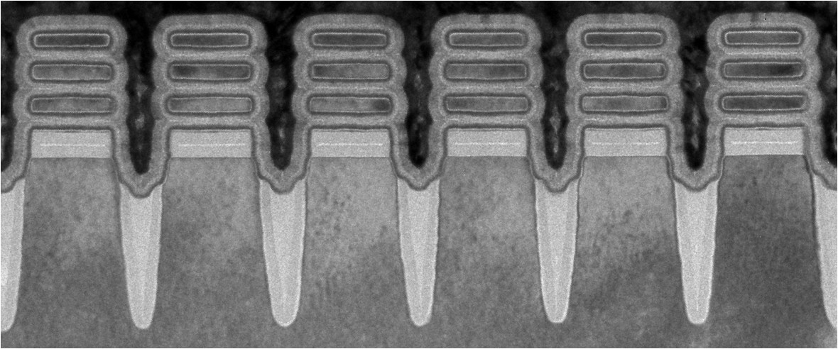
Through the new 2 nm production process that uses nanosheets, chips the size of a fingernail can now fit up to 50 billion transistors. Increasing the number of transistors on a chip allows processor designers to add more ccre-level innovations to boost the computation capabilities for AI, cloud computing, and hardware-enforced security and encryption.
TSMC and Samsung will be using an alternative to nanosheets called gate-all-around FET. This approach will require less money to produce, but it will probably not be as efficient as IBM’s 2 nm nodes, which will be used for industrial and aerospace-grade hardware, anyway.
Source(s)
