 Deutsch
 English
 Español
 Français
 Italiano
 Nederlands
 Polski
 Português
 Русский
 Türkçe
 Svenska
 Chinese
 Magyar
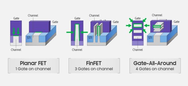
TSMC to implement gate-all-around (GAAFET) transistors on the 2 nm nodes by 2023

TSMC recently announced its plans for the 3 nm nodes that should start mass production by 2H 2022, and it looked like the Taiwanese company was still reluctant to adopt the gate-all-around FET transistors. This would allow Samsung to potentially be the first foundry to bring the new transistor structures to the market in late 2021 with its 3 nm nodes that are said to implement the GAAFET design. Samsung might be rushing here and the yields could turn out subpar, but industry sources cited by DigiTimes claim that TSMC is also accelerating the development of its 2 nm node in order to make it operational ahead of schedule (now planned for mid-2023). These 2 nm nodes will finally make the jump to GAAFET transistors, sources say.
The FinFET transistors will soon be reaching their physical limits, and everything under 3 nm needs to adopt a new transistor design. GAAFET appears to be the only viable solution at this point in time, although scientists found that carbon graphenes could work, as well. Intel tried to implement the GAAFET for its 7 nm CPUs initially scheduled to release next year, but the yields were severely affected and the process needed to be simplified and postponed to 2023. TSMC and Samsung warned Intel that the GAAFET tech is not yet ready for mass production, but this did not stop Samsung to push the launch for its GAAFET 3 nm nodes to late 2021.
DigiTime's sources also suggest that Samsung’s plan to overtake TSMC with the 3 nm GAAFET nodes may fail. This could happen because Samsung’s nodes are historically known to get poorer yields compared to TSMC, so, even though Samsung may have the GAAFET nodes operational in late 2021, the production capacities will probably end up highly restricted, leading to increased production prices, which would not be too appealing to clients like Qualcomm, MediaTek etc. Additionally, Apple secured exclusive production and R&D agreements with TSMC up to the 2 nm nodes.
Source(s)


