 Deutsch
 English
 Español
 Français
 Italiano
 Nederlands
 Polski
 Português
 Русский
 Türkçe
 Svenska
 Chinese
 Magyar
AMD Ryzen 7 PRO 6850HS vs AMD Ryzen 5 7540U vs AMD Ryzen 5 PRO 7540U
AMD Ryzen 7 PRO 6850HS
► remove from comparison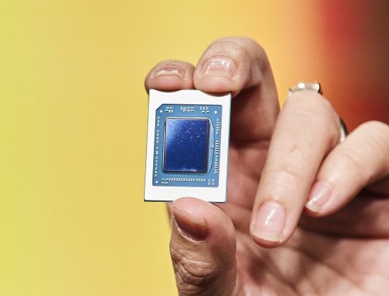
The AMD Ryzen 7 PRO 6850HS is a processor for big (workstation) laptops based of the Rembrandt generation. The R7 6850HS integrates all eight cores based on the Zen 3+ microarchitecture. They are clocked at 3.2 (guaranteed base clock) to 4.7 GHz (Turbo) and support SMT / Hyperthreading (16 threads). The chip is manufactured on the modern 6 nm TSMC process. The HS variant offers a 10 W reduced TDP and therefore a lower sustained performance than the H version. The 6850HS is the professional version of the consumer R7 6800HS with additional management features and the Microsoft Pluton Security processor.
The new Zen 3+ is a refresh of the Zen 3 architecture and should not offer a lot of changes. The chip itself however, offers a lot of new features, like support for USB 4 (40 Gbps), PCI-E Gen 4, DDR5-4800MT/s or LPDDR5-6400MT/s, WiFi 6E, Bluetooth LE 5.2, DisplayPort 2, and AV1 decode.
A big novelty is the integrated GPU Radeon 680M, that is now based on the RDNA2 architecture and offers 12 CUs at up to 2.2 GHz. It should be the fastest iGPU of all at the time of announcement.
Performance
While we have not tested a single system powered by the 6850HS as of August 2023, it's safe to expect the chip to be about as fast as the 6800HS and the 6850H.
Your mileage may vary depending on how high the CPU power limits are and how competent the cooling solution of your system is.
Power consumption
This Ryzen 7 has a default TDP of 35 W (also known as the long-term power limit). Which is way too high to allow it to become a heart of a passively cooled laptop, tablet, mini-PC.
The APU is manufactured on TSMC's 6 nm process leading to great, as of late 2022, energy efficiency.
AMD Ryzen 5 7540U
► remove from comparison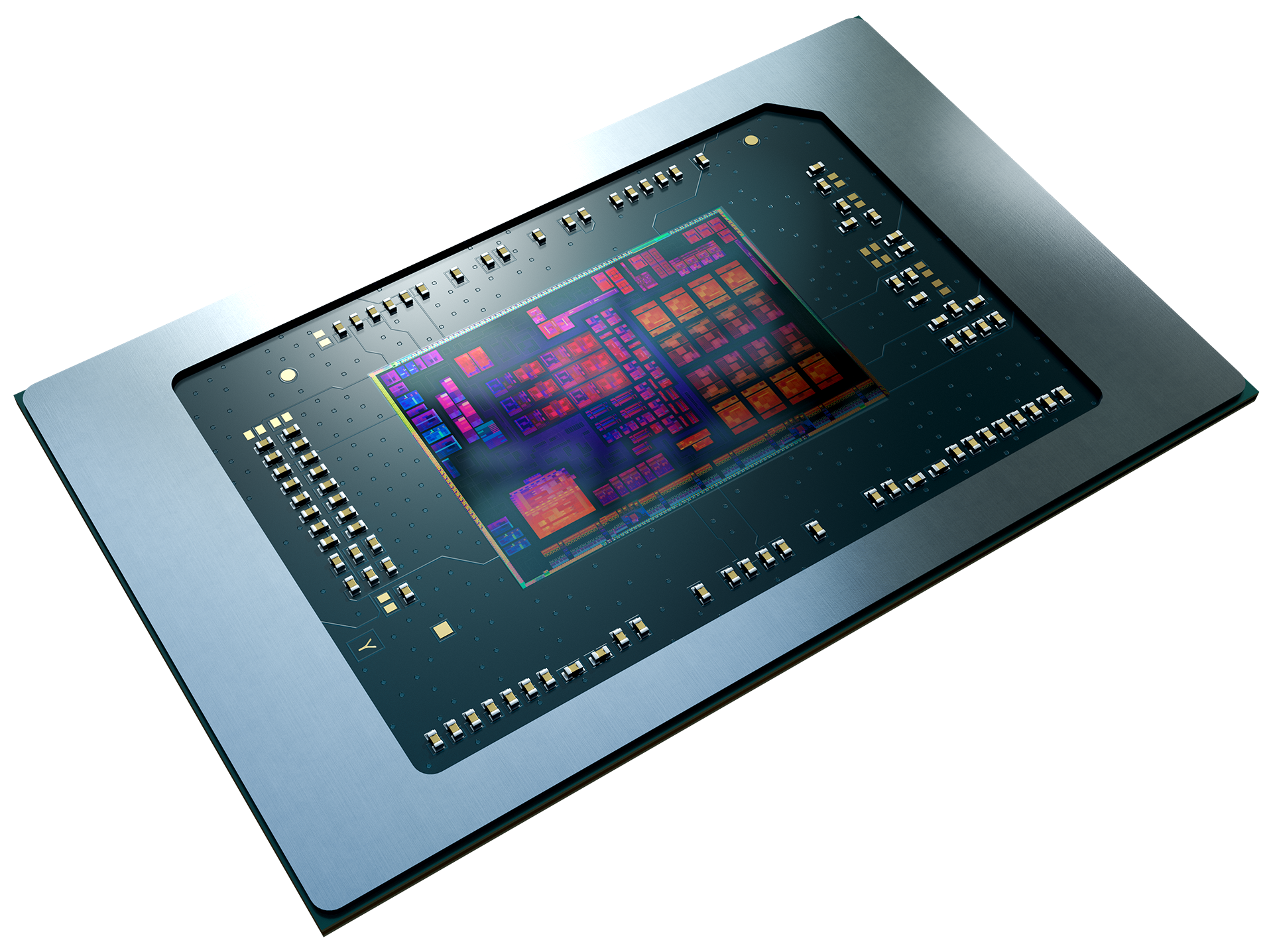
The AMD Ryzen 5 7540U is a fast mid-range laptop processor of the Phoenix series. It offers 6 cores (hexa core) based on the Zen 4 architecture that supports hyperthreading (12 threads). The cores clock from 3.2 (base) up to 4.9 GHz (single core boost). The processor includes 6 MB L2 cache and 16 MB L3 cache.
Thanks to the new Zen 4 architecture and higher clock speeds, the R5 7540U is clearly faster than the old Ryzen 5 6600U (Zen 3, 6 cores, 4.5 GHz). Compared to the similar 7640U, the 7540U offers a lower base clock and a slower iGPU.
The chip integrates a modern and fasts RDNA 3 graphics card (iGPU) called Radeon 740M with 4 of the 12 CUs and 2.5 GHz clock speed. Furthermore, the Phoenix series include a video engine with AV1 de- and encoding and a dual-channel DDR5-5600 / LPDDR5x-7500 memory controller (with ECC support). The new Xilinx FPGA based XDNA AI accelerator (Ryzen AI) is not included in the 7540U. The connectivity features includes 2 possible USB 4 (40 Gbps) ports and 20 PCIe 4.0 lanes for a GPU and SSDs.
The Phoenix series uses a single monolithic design (unlike the chiplet design of the 7045HX series) and is manufactured in the modern 4nm process at TSMC. The TDP can be configured between 15 and 30 Watt (28 Watt default).
AMD Ryzen 5 PRO 7540U
► remove from comparisonThe AMD Ryzen 5 PRO 7540U is a fast mid-range laptop processor of the Phoenix series. It offers 6 cores (hexa core) based on the Zen 4 architecture that supports hyperthreading (12 threads). The cores clock from 3.2 (base) up to 4.9 GHz (single core boost). The processor includes 6 MB L2 cache and 16 MB L3 cache.
Compared to the consumer Ryzen 5 7540U, the PRO models offer additional security, manageability, and reliability features designed for professional users and workstation environments.
Thanks to the new Zen 4 architecture and higher clock speeds, the R5 PRO 7540U is clearly faster than the old Ryzen 5 6600U (Zen 3, 6 cores, 4.5 GHz). Compared to the similar PRO 7640U, the 7540U offers a lower base clock and a slower iGPU.
The chip integrates a modern and fasts RDNA 3 graphics card (iGPU) called Radeon 740M with 4 of the 12 CUs and 2.5 GHz clock speed. Furthermore, the Phoenix series include a video engine with AV1 de- and encoding, a new Xilinx FPGA based XDNA AI accelerator (Ryzen AI) that should be faster than the AI engine in the Apple M2 SOC and a dual-channel DDR5-5600 / LPDDR5x-7500 memory controller (with ECC support). The connectivity features includes 2 possible USB 4 (40 Gbps) ports and 20 PCIe 4.0 lanes for a GPU and SSDs.
The Phoenix series uses a single monolithic design (unlike the chiplet design of the 7045HX series) and is manufactured in the modern 4nm process at TSMC. The TDP can be configured between 35 and 45 Watt.
| Model | AMD Ryzen 7 PRO 6850HS | AMD Ryzen 5 7540U | AMD Ryzen 5 PRO 7540U | ||||||||||||||||||||||||||||||||||||||||||||||||||||||||||||||||||||||||
| Series | AMD Rembrandt (Zen 3+) | AMD Phoenix (Zen 4, Ryzen 7040) | AMD Phoenix (Zen 4, Ryzen 7040) | ||||||||||||||||||||||||||||||||||||||||||||||||||||||||||||||||||||||||
| Codename | Rembrandt-HS (Zen 3+) | Phoenix (Zen4) | Phoenix (Zen4) | ||||||||||||||||||||||||||||||||||||||||||||||||||||||||||||||||||||||||
| Series: Phoenix (Zen 4, Ryzen 7040) Phoenix (Zen4) |
|
|
| ||||||||||||||||||||||||||||||||||||||||||||||||||||||||||||||||||||||||
| Clock | 3200 - 4700 MHz | 3200 - 4900 MHz | 3200 - 4900 MHz | ||||||||||||||||||||||||||||||||||||||||||||||||||||||||||||||||||||||||
| L1 Cache | 512 KB | 384 KB | 384 KB | ||||||||||||||||||||||||||||||||||||||||||||||||||||||||||||||||||||||||
| L2 Cache | 4 MB | 6 MB | 6 MB | ||||||||||||||||||||||||||||||||||||||||||||||||||||||||||||||||||||||||
| L3 Cache | 16 MB | 16 MB | 16 MB | ||||||||||||||||||||||||||||||||||||||||||||||||||||||||||||||||||||||||
| Cores / Threads | 8 / 16 | 6 / 12 6 x 4.9 GHz AMD Zen 4 | 6 / 12 6 x 4.9 GHz AMD Zen 4 | ||||||||||||||||||||||||||||||||||||||||||||||||||||||||||||||||||||||||
| TDP | 35 Watt | 28 Watt | 15 Watt | ||||||||||||||||||||||||||||||||||||||||||||||||||||||||||||||||||||||||
| Technology | 6 nm | 4 nm | 4 nm | ||||||||||||||||||||||||||||||||||||||||||||||||||||||||||||||||||||||||
| max. Temp. | 95 °C | 100 °C | 100 °C | ||||||||||||||||||||||||||||||||||||||||||||||||||||||||||||||||||||||||
| Socket | FP7/FP7r2 | ||||||||||||||||||||||||||||||||||||||||||||||||||||||||||||||||||||||||||
| Features | DDR5-4800/LPDDR5-6400 RAM (incl. ECC), PCIe 4, PRO, MMX, SSE, SSE2, SSE3, SSSE3, SSE4A, SSE4.1, SSE4.2, AVX, AVX2, BMI2, ABM, FMA, ADX, SMEP, SMAP, SMT, CPB, AES-NI, RDRAND, RDSEED, SHA, SME | ||||||||||||||||||||||||||||||||||||||||||||||||||||||||||||||||||||||||||
| iGPU | AMD Radeon 680M ( - 2200 MHz) | AMD Radeon 740M ( - 2500 MHz) | AMD Radeon 740M ( - 2500 MHz) | ||||||||||||||||||||||||||||||||||||||||||||||||||||||||||||||||||||||||
| Architecture | x86 | x86 | x86 | ||||||||||||||||||||||||||||||||||||||||||||||||||||||||||||||||||||||||
| Announced | |||||||||||||||||||||||||||||||||||||||||||||||||||||||||||||||||||||||||||
| Manufacturer | www.amd.com | www.amd.com | www.amd.com | ||||||||||||||||||||||||||||||||||||||||||||||||||||||||||||||||||||||||
| Die Size | 178 mm2 | 178 mm2 |

Benchmarks
* Smaller numbers mean a higher performance
1 This benchmark is not used for the average calculation