During the opening keynote demonstration, Intel stressed the orders of magnitude reduction in power from the jump to the new generation Haswell CPUs compared to the current "tick" platform. How have engineers gone about in achieving the feat?
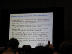
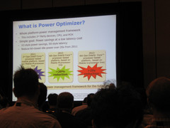
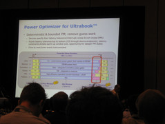
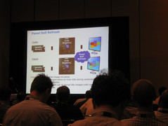
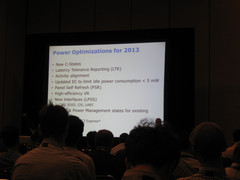
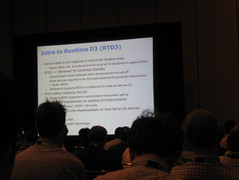
A separate session was dedicated solely to power management strategies on the Haswell architecture. Perhaps unsurprisingly, the optimizations to power requirements weren't only done on the CPU side, but mostly on the entire chipset and motherboard themselves. Intel wanted to see how low of a power state multiple key areas can reduce to without suffering performance or latency issues. As a result, new standards have been set across bus interconnects, SATA, USB 2.0, USB 3.0, WLAN, and even DisplayPort chipsets specifically for running on low-power states. Standyby performance enhancements, increased tolerance to power changes, and Runtime D3 (RD3) round up many of the hardware strategies necessary to reach the claimed 20x reduction in power.
As for the software side, BLA (Battery Life Analyzer) will monitor overheads, HDD spindown towns, memory bandwidth usage and track system utilization to study power consumption on a case-by-case basis.
Together, a typical idling SoC can draw only 90 mW compared to 2 W of current generation platforms. Battery life will increase as expected, but by exactly how long was never mentioned.


