Deposition breakthrough enables the development of 120-layer high-density 3D DRAM
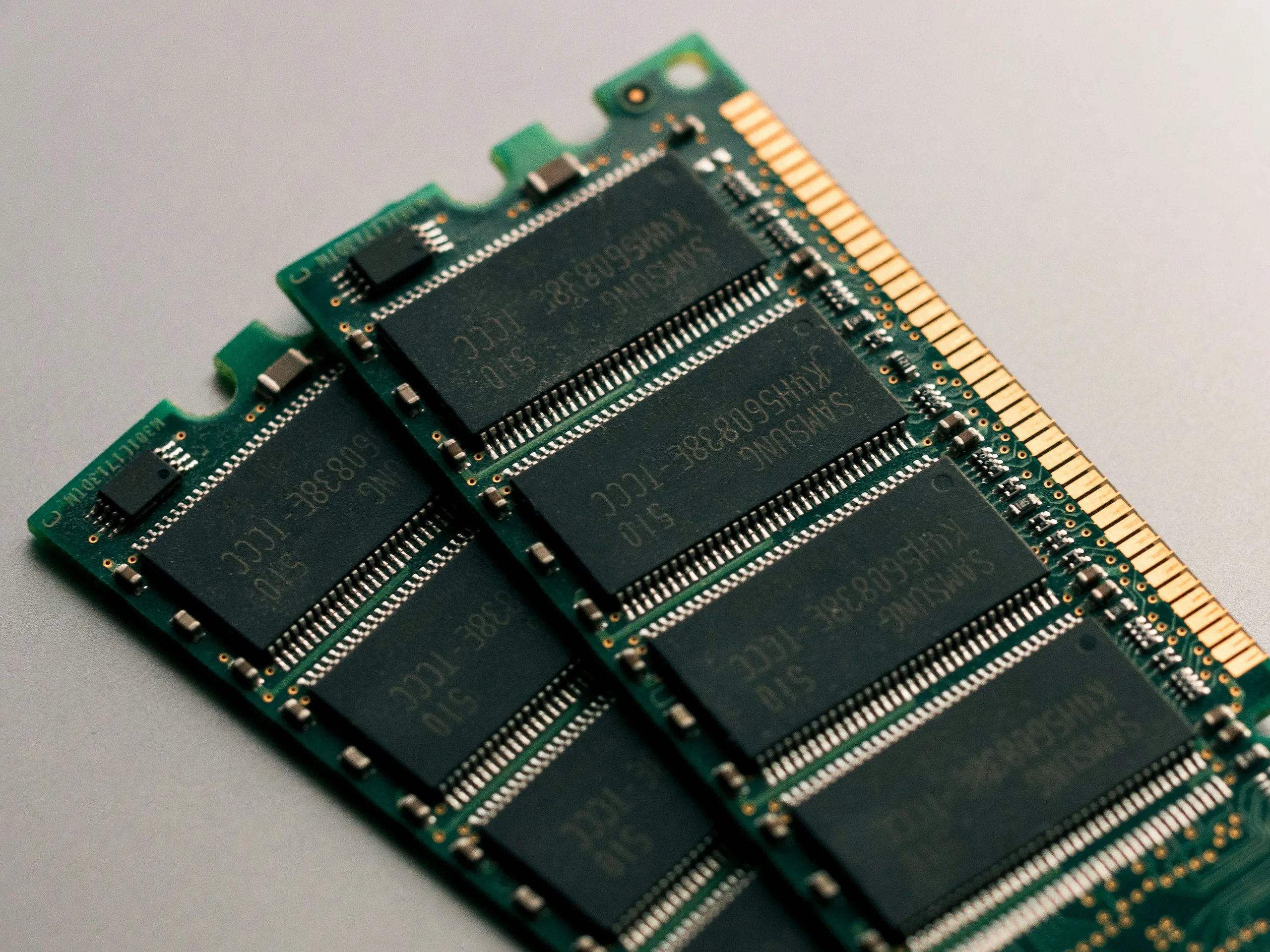
Researchers at imec and Ghent University have demonstrated a method for growing 120 alternating layers of silicon and silicon-germanium on 300mm wafers to support the development of three-dimensional DRAM. Each stack consists of about 65 nanometers of silicon and 10 nanometers of silicon-germanium with 20 percent germanium, repeated 120 times. The inner wafer stays fully strained, which is important for device yield. Most misfit dislocations appear near the wafer edge, where the bevel facilitates relaxation.
Creating these channels requires silicon-germanium layers that can be selectively etched, which is why they chose a 20 percent germanium composition. The team’s results demonstrate that building more than 100 bilayers is feasible on production-size wafers, enabling higher memory density.
To achieve this, the team adjusted its process to keep interfaces sharp and limit mixing between layers, while still maintaining good throughput. They used reduced-pressure CVD in ASM Intrepid tools, growing silicon with silane at about 675 degrees Celsius and silicon-germanium with dichlorosilane and germane. Secondary-ion mass spectrometry compared a normal stack to one kept hot for as long as 60 extra bilayers would take. The germanium profiles matched, showing that there was very little mixing between silicon and silicon-germanium under these conditions.
Managing defects was also critical. High-resolution X-ray diffraction and cross-sectional TEM showed that the superlattice inside the wafer stayed fully strained, with no threading dislocations found there. Although the total silicon-germanium thickness is approximately 1.2 micrometers, significantly more than the usual critical thickness for a single layer, the multilayer design and clean growth allowed it to remain stable. Where strain is relaxed, near the edge, the authors attribute this to the bevel effect and suggest reducing lattice mismatch by lowering the germanium content or adding a small amount of carbon. They also monitored wafer bow and, when necessary, applied a compressive nitride layer to the back, after protecting the front side.
Uniformity challenges in layer deposition were a key focus for the team. The paper connects changes in layer thickness and non-uniformity in thick stacks to temperature shifts caused by unwanted buildup on the reactor’s quartz tube, which affects how the lamps heat the chamber. A newer tool with active temperature control for the tube reduced this drift, improving both side-to-side uniformity and consistency between layers. For comparison, optimized single-layer runs had thickness variations under about 1.3 percent, while very thick cap structures increased that to about 1.8 percent, with the edge being most sensitive. The analysis reports interface thicknesses on the order of a few nanometers, with bottom-of-stack interfaces around ~2.6–2.9 nanometers and sharper transitions higher up, consistent with reduced segregation and interdiffusion at the chosen temperature and chemistry. These microscopy results align with x-ray satellite peaks that remain well-resolved and vertically aligned with the substrate peak, another indicator of a coherent, strained superlattice.
Source(s)
AIP (in English)
