

Intel Core Ultra 5 245HX vs AMD Ryzen 7 8840HX vs AMD Ryzen 9 8940HX
Intel Core Ultra 5 245HX
► remove from comparisonThe Intel Core Ultra 5 245HX is a fast mid-range mobile CPU for gaming notebooks based on the Arrow Lake architecture. It offers 20 cores consisting of 6 of the 8 fast performance cores with up to 5.1 GHz and 8 of the 16 smaller efficiency cores with up to 4.5 GHz clock speed. The CPU can access 24 MB L2 cache and 26 MB L3 cache and is specified with a TDP of 55 watts.
The SoC integrates a small dedicated NPU called AI Boost with 13 TOPS (Int8) and optionally supports vPro Enterprise. The integrated memory controller supports up to 192 GB DDR5-6400 (dual channel, ECC optional). The integrated GPU (iGPU) is a small graphics card called Intel Graphics, which offers three of the four Xe cores with 300 - 1900 MHz.
Performance - High End
Thanks to the improved IPC of the cores (especially the efficiency cores), the CPU should be just before or at the level of the Raptor Lake Core i9-14500HX (6 + 8 cores, max 5 / 3.5 GHz). This makes the CPU very suitable for demanding tasks such as high-end gaming (2024 games) and content creation.
Production - TSMC and Foveros
The Arrow Lake-HX chips are based on the desktop Arrow Lake-S chips and are composed of several chiplets. The CPU part is manufactured at TSMC in the modern N3B (3nm) process, the GPU also comes from TSMC in the N5P process. The SoC and I/O tile are manufactured in the TSMC N6 process. The base tile is manufactured by Intel in the 22nm process and carries the individual chiplets thanks to Fovero's 3D packaging.
AMD Ryzen 7 8840HX
► remove from comparison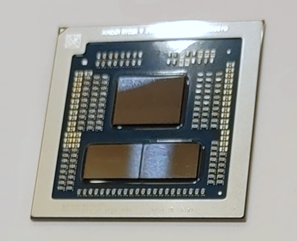
The AMD Ryzen 7 8840HX is a higher-end 12-core Dragon Range refresh lineup processor that debuted in April 2025 and is primarily targeted at gaming laptops. The product offers 12 SMT-enabled Zen 4 cores (24 threads) running at 2.9 GHz to 5.1 GHz, along with a rather basic Radeon 610M RDNA 2 architecture iGPU. This Ryzen 7 8000 APU is essentially a Ryzen 9 7845HX with the base clock speed and Turbo clock speed cut by 100 MHz each.
The 8840HX is composed of three dies made on two different nodes (5 nm for CPU cores; 6 nm for other componentry). It features a very healthy 28 PCIe 5 lanes for connecting graphics cards and SSDs as fast as 15.75 GB/s. The RAM controller is limited to DDR5-5200 or slower; there is no NPU and no Thunderbolt support, the product page on amd.com indicates, but the clock multiplier is unlocked for easy overclocking.
Performance
While we have not tested a single system featuring the 8840HX as of April 2025, we can take the 7845HX's multi-thread Cinebench scores and lower them by a percent or two. If we do that, the 8840HX emerges as a Core i7-14650HX and Core i7-14700HX-beating CPU which is fast enough for any 2025 or 2026 game.
Power consumption
Much like the 7845HX, the 8840HX has a base TDP (long-term power limit) of 55 watts that can officially be jacked up to as high as 75 watts. In fact, Alienware allows the 7845HX to consume well over 100 watts in its 2023 Alienware m16 (the only 7845HX system Notebookcheck has tested). Either way, to dissipate 50+ watts, at least one high-RPM fan is needed.
AMD Ryzen 9 8940HX
► remove from comparisonThe AMD Ryzen 9 8940HX is a flagship 16-core Dragon Range refresh lineup laptop processor that debuted in April 2025. The product offers 16 SMT-enabled Zen 4 cores (32 threads) running at 2.4 GHz to 5.3 GHz, along with a rather basic Radeon 610M RDNA 2 architecture iGPU. This Ryzen 9 8000 APU is essentially a Ryzen 9 7940HX with the Turbo clock speed increased by 100 MHz.
The 8940HX is composed of three dies made on two different nodes (5 nm for CPU cores; 6 nm for other componentry). It features a very healthy 28 PCIe 5 lanes for connecting graphics cards and SSDs as fast as 15.75 GB/s. The RAM controller is limited to DDR5-5200 or slower; there is no NPU and no Thunderbolt support, the product page on amd.com indicates, but the clock multiplier is unlocked for easy overclocking.
Performance
While we have not tested a single system featuring the 8940HX as of April 2025, we do have some Cinebench benchmark scores for the 7940HX. Based on those, the newer Ryzen 9 should have no trouble beating the Core i9-13950HX, Core i9-13980HX and Core i9-14900HX.
That being said, with this many cores the APU will probably do a much better job serving content creators rather than gamers.
Power consumption
Much like the 7940HX, the 8940HX has a base TDP (long-term power limit) of 55 watts that can officially be jacked up to as high as 75 watts. To dissipate 50+ watts, at least one high-RPM fan is needed.
| Model | Intel Core Ultra 5 245HX | AMD Ryzen 7 8840HX | AMD Ryzen 9 8940HX | ||||||||||||||||||||||||||||||||||||||||||||||||||||||||
| Codename | Arrow Lake-HX | Dragon Range refresh (Zen 4) | Dragon Range refresh (Zen 4) | ||||||||||||||||||||||||||||||||||||||||||||||||||||||||
| Series | Intel Arrow Lake | AMD Dragon Range (Zen 4, Ryzen 7X4X/8X4X) | AMD Dragon Range (Zen 4, Ryzen 7X4X/8X4X) | ||||||||||||||||||||||||||||||||||||||||||||||||||||||||
| Series: Dragon Range (Zen 4, Ryzen 7X4X/8X4X) Dragon Range refresh (Zen 4) |
|
|
| ||||||||||||||||||||||||||||||||||||||||||||||||||||||||
| Clock | 2600 - 5100 MHz | 2900 - 5100 MHz | 2400 - 5300 MHz | ||||||||||||||||||||||||||||||||||||||||||||||||||||||||
| L2 Cache | 24 MB | 12 MB | 16 MB | ||||||||||||||||||||||||||||||||||||||||||||||||||||||||
| L3 Cache | 26 MB | 64 MB | 64 MB | ||||||||||||||||||||||||||||||||||||||||||||||||||||||||
| Cores / Threads | 14 / 14 6 x 5.1 GHz Intel Lion Cove P-core 8 x 4.5 GHz Intel Skymont E-core | 12 / 24 12 x 5.1 GHz AMD Zen 4 | 16 / 32 16 x 5.3 GHz AMD Zen 4 | ||||||||||||||||||||||||||||||||||||||||||||||||||||||||
| TDP | 55 Watt | 55 Watt | 55 Watt | ||||||||||||||||||||||||||||||||||||||||||||||||||||||||
| TDP Turbo PL2 | 160 Watt | ||||||||||||||||||||||||||||||||||||||||||||||||||||||||||
| Technology | 3 nm | CCD = 5nm, I/O = 6 nm | CCD = 5nm, I/O = 6 nm | ||||||||||||||||||||||||||||||||||||||||||||||||||||||||
| iGPU | Intel Arc Graphics 3-core GPU (Arrow Lake) (300 - 1900 MHz) | AMD Radeon 610M ( - 2200 MHz) | AMD Radeon 610M ( - 2200 MHz) | ||||||||||||||||||||||||||||||||||||||||||||||||||||||||
| Architecture | x86 | x86 | x86 | ||||||||||||||||||||||||||||||||||||||||||||||||||||||||
| Announced | |||||||||||||||||||||||||||||||||||||||||||||||||||||||||||
| Manufacturer | www.intel.com | www.amd.com | amd.com | ||||||||||||||||||||||||||||||||||||||||||||||||||||||||
| L1 Cache | 768 KB | 1 MB | |||||||||||||||||||||||||||||||||||||||||||||||||||||||||
| max. Temp. | 100 °C | ||||||||||||||||||||||||||||||||||||||||||||||||||||||||||
| Socket | FL1 | FL1 | |||||||||||||||||||||||||||||||||||||||||||||||||||||||||
| Features | DDR5-5200 RAM, PCIe 5, MMX, SSE, SSE2, SSE3, SSSE3, SSE4A, SSE4.1, SSE4.2, AVX, AVX2, AVX-512, BMI2, ABM, FMA, ADX, SMEP, SMAP, SMT, CPB, AES-NI, RDRAND, RDSEED, SHA, SME | DDR5-5200 RAM, PCIe 5, MMX, SSE, SSE2, SSE3, SSSE3, SSE4A, SSE4.1, SSE4.2, AVX, AVX2, AVX-512, BMI2, ABM, FMA, ADX, SMEP, SMAP, SMT, CPB, AES-NI, RDRAND, RDSEED, SHA, SME |

Benchmarks

Average Benchmarks AMD Ryzen 9 8940HX → 0% n=0
* Smaller numbers mean a higher performance
1 This benchmark is not used for the average calculation