Less than 1 nm: New technology makes tiny chips possible

How small something can be built depends on how small the associated building blocks are. A silicon atom, for example, measures 117 picometers or 0.000000000117 meters. That's not much, but the current smallest resolution of the 3-nanometer production process is just 26 times this value.
At some point, the structure will therefore become too fine to guarantee a reliable structure for a transistor. A research group at the Institute for Basic Science in Daejeon, South Korea, has nevertheless succeeded in skipping several generations of chip development with the help of a new approach.
Currently, the desired structure is gradually printed on light-sensitive surfaces in wafer-thin layers in the form of photolithography. However, this is only possible with a thickness of several atoms.
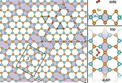
In order to circumvent the technical limits of the lithography process, the defect in a crystal structure is used as a gate instead. The researchers found what they were looking for between mirrored structures of two-dimensional molybdenum disulfide crystals.
This is precisely where a one-dimensional gap of just 0.4 nanometers, i.e. 400 picometers or barely more than three silicon atoms, is created. By building such a structure molecule by molecule, it was possible to make it almost ten times smaller than previously possible.
Based on this size, a transistor with a length of 3.9 nanometers could be constructed, albeit currently only in theory. This corresponds to one-sixth of the 3-nanometer manufacturing process, or one-thirtieth of the surface area.
Depending on when a technical implementation can be achieved, the chip development timetable could receive a major boost. While 2 nanometers should be achieved by 2025, it was assumed that a resolution of 0.5 nanometers could not be achieved until 2037.
Moore's Law could therefore continue to apply for quite some time.
Source(s)
