IBM's concept chip can transfer a terabit of data per second
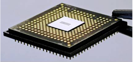
Recently IBM researchers have built a prototype optical chip which is capable of transferring a terabyte of data per second which is unveiled at the Optical Fiber Communication Conference in Los Angeles. This chip has an innovative design with 48 holes drilled into the standard CMOS chip, facilitating the movement of light. This fast chip will be even more power efficient and is based on the so called Holey Optochip technology.
Optical chips which are generally used in today’s supercomputers and in IBM systems such as Power 775 and Blue Gene, moves data with light instead of electrons. According to Clint Schow, IBM optical Links Group manager, the optical technology is mostly favored over electrical for transmitting high-bandwidth data over long distances and so are used in telecommunication networks.
He also mentions that we hardly had a supercomputer using optics ten years ago but we are seeing large scale deployments, mostly for rack-to-rack interconnects within supercomputers. He also added that it's making a way deeper into the system and getting closer to the actual processor. He also said that their target is the bandwidth that interconnects different processors in the system, not the processor talking to its memory, but a processor talking to another processor in a large parallel system.
The Holey Optochip uses 4.7 watts in delivering about one trillion bits per second which will be enough to download 500 HD movies. The chip’s dimension is only about 5.2mm by 5.8mm which is about one eighth of a dime.
According to Schow, the chip is being made of a single CMOS, plain-Jane unmodified process chip. The base of the chip has all the electronic circuit functions to complete the optical link. It has drivers that modulate vertical cavity lasers and receiver circuits that convert photocurrent from a detector into a usable electrical signal.
IBM has also used 850-nanometer vertical cavity surface emitting lasers and photodiode arrays, by drilling holes into the chip and both soldered onto the chip. The holes are for optical access through the back of the chip to the transmitter and receiver channels.
The current optical chips that are being used includes 12 channels each moving 10Gigabits per second, while the Holey Optochip has 48 channels each moving 20 Gigabits per second for a total of 960 Gigabits, which is just below a terabit.
The chip is also called to be as more power efficient as it transmits much more data which lead to better efficiency as measured in watts per bit. The speed of each channel is also expected to be raised further to about 25 Gigabits per second in the near future.
Later Schow also added that although IBM itself won’t be mass producing the chips but they could probably be commercially available within a year or two. The price for the chip could be in the range of $100 to $200 as he expects.