

Google Tensor vs Unisoc T9100 (T820) vs UNISOC T8200 (T765)
Google Tensor
► remove from comparison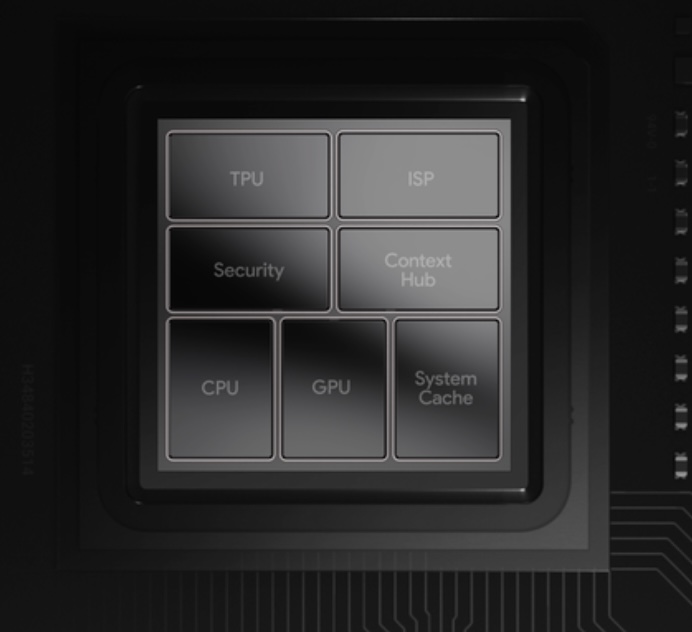
The Google Tensor SoC (G1, first generation) is the first smartphone processor from Google. It is positioned as a high end SoC and focuses on the integrated TPU for efficient AI and ML calculations. The CPU part integrates two fast and big ARM Cortex X1 cores at up to 2.8 GHz. A second cluster integrates 2 mid range Cortex-A76 cores at up to 2.25 GHz. Finally, four small ARM Cortex-A55 cores with up to 1.8 GHz are integrated for efficiency purposes. All cores can access the shared 4 MB L3 cache.
The successors of the Tensor SoC are the Tensor G2 and G3.
The chip also integrates a Titan M2 security processor and a ARM Mali G78 MP20 GPU. The chip is manufactured in the modern 5nm process.
Unisoc T9100 (T820)
► remove from comparison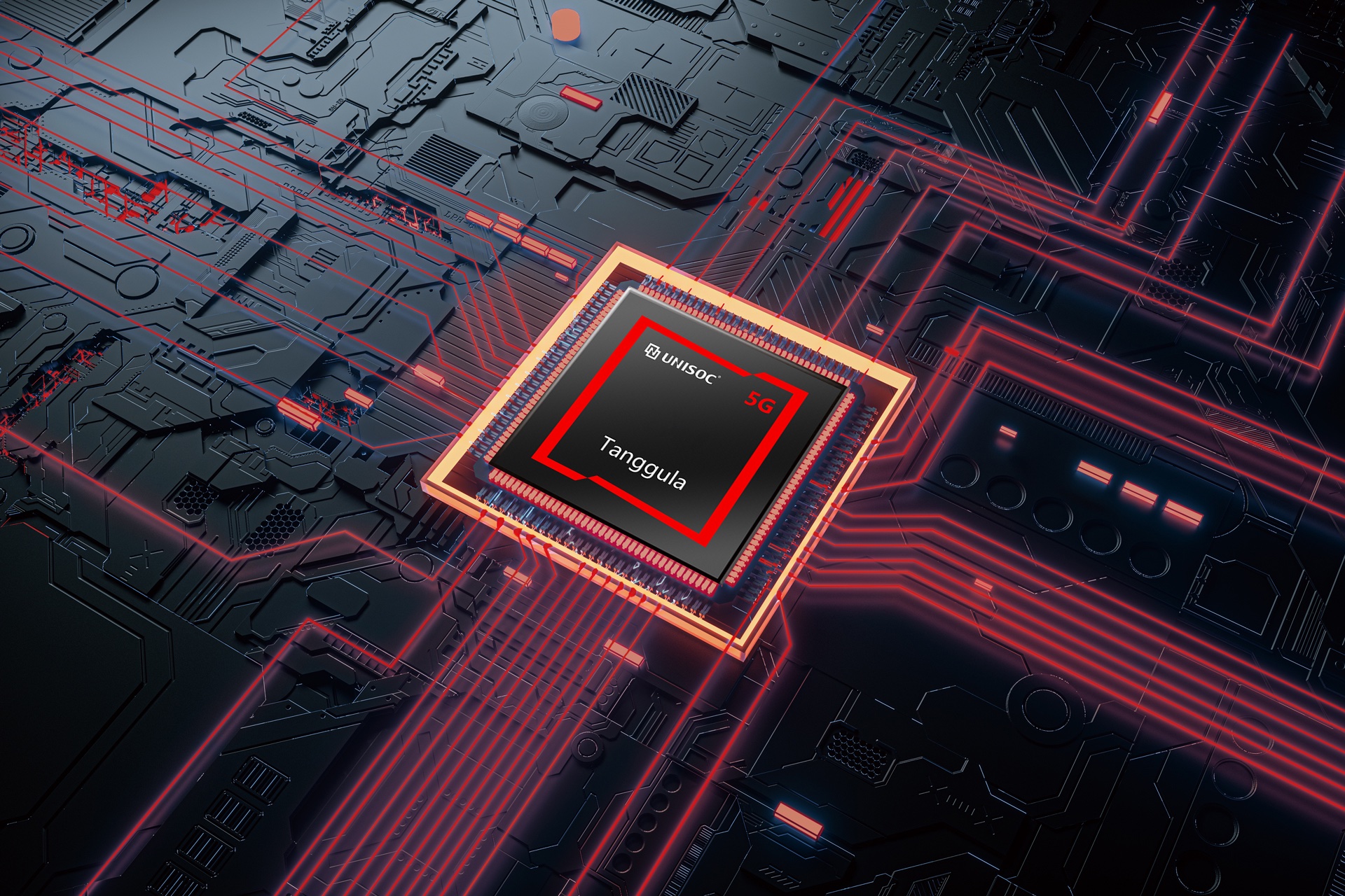
The Unisoc T9100 (formely Unisoc T820) is a mid range SoC for Android based smartphones and tablets. It integrates an octa-core CPU with three clusters. One fast ARM Cortex-A76 clocked at up to 2.7 GHz, three more A76 performance cores clocked at up to 2.3 GHz and a power efficiency cluster of four ARM-Cortex-A55 cores with up to 2.1 GHz. The integrated memory controller supports LPDDR4/4X with up to 2133 MHz (2x 16 Bit). The integrated ISP supports two main cameras and two subsidiary cameras (up to 108 MPix). The integrated graphics card is an ARM Mali-G57 MC4 (4 cores) at up to 850 MHz. Unisoc also specifies that the T9100 offers hardware AI acceleration with up to 8.0 TOPS peak performance of the NPU.
The chip is manufactured on the modern 6nm EUV process.
UNISOC T8200 (T765)
► remove from comparison
The UniSoc T8200 (former UniSoc T765) is a mid-range SoC with 8 processor cores in two clusters. The two large ARM Cortex-A76 cores are clocked at up to 2.3 GHz. The six smaller cores run at up to 2.1 GHz.
The integrated memory controller supports LPDDR4/4X with up to 2133 MHz (2x 16 bit). The integrated ISP supports a camera up to 108 MPixel. The integrated graphics card is an ARM Mali-G57 MC2 (2 cores) is used. The built-in 5G modem supports TDD+FDD CA in the sub-6GHz spectrum with 130 MHz bandwidth.
The chip is manufactured using the somewhat older 6nm process (EUV at TSMC).
| Model | Google Tensor | Unisoc T9100 (T820) | UNISOC T8200 (T765) |
| Codename | Exynos X1 / Cortex-A76 / A55 | Cortex-A76 / A55 | Cortex-A76 / A55 |
| Clock | 1800 - 2800 MHz | 2100 - 2700 MHz | 2100 - 2300 MHz |
| L3 Cache | 4 MB | ||
| Cores / Threads | 8 / 8 | 8 / 8 | 8 / 8 2 x 2.3 GHz ARM Cortex-A76 6 x 2.1 GHz ARM Cortex-A55 |
| Technology | 5 nm | 6 nm | 6 nm |
| Features | ARM Mali-G78MP20 GPU | ISP (2 main + 2 subsidiary, 108M 9-in-1, 64M ZSL) | ISP (2 main + 2 subsidiary, 108M 4-in-1, 64M ZSL) |
| iGPU | ARM Mali-G78 MP20 ( - 848 MHz) | ARM Mali-G57 MP4 ( - 850 MHz) | ARM Mali-G57 MP2 ( - 850 MHz) |
| Architecture | ARM | ARM | ARM |
| Announced | |||
| Manufacturer | blog.google |
Benchmarks
Average Benchmarks Google Tensor → 100% n=2
Average Benchmarks Unisoc T9100 (T820) → 70% n=2
Average Benchmarks UNISOC T8200 (T765) → 57% n=2
* Smaller numbers mean a higher performance
1 This benchmark is not used for the average calculation