 Deutsch
 English
 Español
 Français
 Italiano
 Nederlands
 Polski
 Português
 Русский
 Türkçe
 Svenska
 Chinese
 Magyar
Intel Core i7-1068G7 vs AMD Ryzen 5 4680U
Intel Core i7-1068G7
► remove from comparisonThe Intel Core i7-1068G7 is a quad-core SoC for laptops and Ultrabooks based on the Ice-Lake-U generation that was announced in Mai 2019 (Computex). It integrates four Sunnycove processor cores (8 threads thanks to HyperThreading) clocked at 2.3 (base) - 4.1 (single core Turbo) GHz. All four cores can run at up to 3.6 GHz using Turbo Boost. According to Intel the Sunnycove cores achieve 18% more IPCs (Instructions per Clock) and therefore the CPU performance should be similar to the higher clocked Whiskey-Lake and Coffee-Lake predecessors (e.g. Core i7-8559U, 2.7 - 4.5 GHz). The Core i7-1068G7 is the fastest and only 28 Watt Ice Lake-U chip at the time of announcement in 2019.
The biggest improvement for Ice-Lake is the integrated Gen 11 graphics card called Iris Plus Graphics. The Core i7-1065G7 integrates the biggest G7 variant with 64 CUs clocked at 300 - 1100 MHz. The Iris Plus G7 should be twice as fast as the predecessors and best the AMD Vega 10 GPU in current Ryzen APUs.
Other improvements for Ice Lake are the AI hardware acceleration and the partial integration of Thunderbolt and Wifi 6 in the chip. The integrated DDR4 memory controller supports modules with up to 3200 MHz (and LPDDDR4 3733).
The Core i7-1068G7 is produced in the new 10nm process at Intel that should offer a comparable performance to the 7nm process at TSMC. The TDP is specified at 28 Watts and therefore the CPU is best used in small multimedia laptops from 13-inch upwards (e.g. like a MacBook Pro 13).
AMD Ryzen 5 4680U
► remove from comparison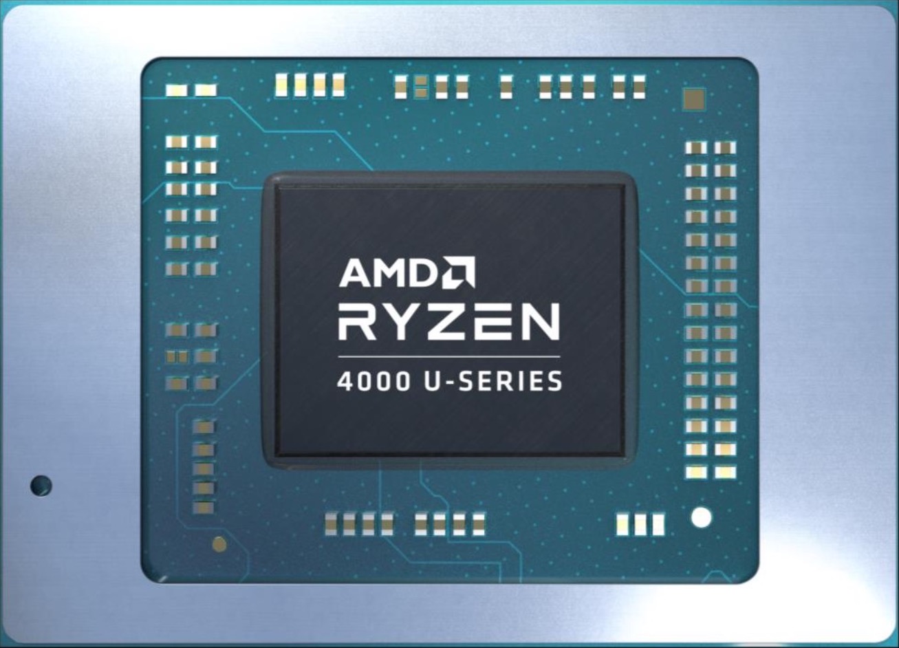
The AMD Ryzen 5 4680U is a semi-custom APU of the Renoir family designed for Microsoft devices. The 4680U integrates six CPU cores based on the Zen 2 microarchitecture clocked at 2.2 GHz (base) to 4 GHz (Boost) with SMT support for a total 12 threads. The two advantages a 4680U has over the older Ryzen 5 4600U are its higher base clock speed and a faster iGPU.
Architecture
The chip is manufactured on the modern 7 nm TSMC process and in part thanks to this fact, AMD advertises a 2x performance per watt improvement over the 12 nm Ryzen 3000 mobile processors. The built-in dual-channel memory controller supports LPDDR4-4266 RAM. Furthermore, 8 MB of L3 cache can be found on the chip.
Just like the other mobile Ryzen 4000 CPUs, a 4680U supports PCI-Express 3.0. Please go to our Renoir processor hub page for additional information on the product family.
Performance
Multi-thread performance is most comparable to the Ryzen 7 4700U and the Core i5-10500H, the latter being a much more power-hungry chip. This makes the Ryzen a more than decent CPU for most tasks, as of early 2022.
Graphics
In addition to the six CPU cores, the APU also integrates a DX 12 compatible Radeon RX Vega 7 graphics adapter with 7 CUs (448 unified shaders) at up to 1,500 MHz. The Vega iGPU will have no trouble HW-decoding AVC, HEVC and VP9 videos, but the newer AV1 codec will only be decoded via software. In terms of gaming, we are looking at an MX150-level performance. Pretty much all games released in 2020 can be played on low to medium settings in 720p on this graphics adapter.
Power consumption
This Ryzen 5 series chip has a default TDP (also known as the long-term power limit) of 15 W, a value that laptop makers - Microsoft, in this case - are free to change to anything between 10 W and 25 W, with clock speeds and performance changing accordingly as a result. Indeed, we saw the CPU consume roughly 23 watts when subjected to our usual stress testing routine.
The 7 nm TSMC process this Ryzen is built with makes for very decent, as of mid 2022, energy efficiency.
| Model | Intel Core i7-1068G7 | AMD Ryzen 5 4680U | ||||||||||||||||||||||||||||||||||||
| Series | Intel Ice Lake | AMD Renoir (Ryzen 4000 APU) | ||||||||||||||||||||||||||||||||||||
| Codename | Ice Lake U | Renoir-U (Zen 2) | ||||||||||||||||||||||||||||||||||||
| Series: Renoir (Ryzen 4000 APU) Renoir-U (Zen 2) |
|
| ||||||||||||||||||||||||||||||||||||
| Clock | 2300 - 4100 MHz | 2200 - 4000 MHz | ||||||||||||||||||||||||||||||||||||
| L1 Cache | 192 KB | 384 KB | ||||||||||||||||||||||||||||||||||||
| L2 Cache | 2 MB | 3 MB | ||||||||||||||||||||||||||||||||||||
| L3 Cache | 8 MB | 8 MB | ||||||||||||||||||||||||||||||||||||
| Cores / Threads | 4 / 8 | 6 / 12 | ||||||||||||||||||||||||||||||||||||
| TDP | 28 Watt | 15 Watt | ||||||||||||||||||||||||||||||||||||
| Technology | 10 nm | 7 nm | ||||||||||||||||||||||||||||||||||||
| Features | AVX512, DL Boost, Turbo Boost 2.0 | LPDDR4-4266 RAM, PCIe 3, MMX, SSE, SSE2, SSE3, SSSE3, SSE4A, SSE4.1, SSE4.2, AVX, AVX2, BMI2, ABM, FMA, ADX, SMEP, SMAP, SMT, CPB, AES-NI, RDRAND, RDSEED, SHA | ||||||||||||||||||||||||||||||||||||
| iGPU | Intel Iris Plus Graphics G7 (Ice Lake 64 EU) (300 - 1100 MHz) | AMD Radeon RX Vega 7 ( - 1500 MHz) | ||||||||||||||||||||||||||||||||||||
| Architecture | x86 | x86 | ||||||||||||||||||||||||||||||||||||
| Announced | ||||||||||||||||||||||||||||||||||||||
| max. Temp. | 105 °C | |||||||||||||||||||||||||||||||||||||
| Socket | FP6 | |||||||||||||||||||||||||||||||||||||
| Manufacturer | www.amd.com |
