 Deutsch
 English
 Español
 Français
 Italiano
 Nederlands
 Polski
 Português
 Русский
 Türkçe
 Svenska
 Chinese
 Magyar
Intel Core i5-1034G1 vs AMD Ryzen 9 4900HS
Intel Core i5-1034G1
► remove from comparisonThe Intel Core i5-1034G1 is a power efficient quad-core SoC for laptops and Ultrabooks based on the Ice -Lake-U generation that was announced in Mai 2019 (Computex). It integrates four Sunnycove processor cores (8 threads thanks to HyperThreading) clocked at 0.8 (base) - 3.6 (single core Turbo) GHz. 2 cores can reach 3.6 GHz and all four 3.3 GHz using Turbo Boost. According to Intel the Sunnycove cores achieve 18% more IPCs (Instructions per Clock) and therefore the CPU performance should be similar to the higher clocked Whiskey-Lake predecessors (e.g. Core i5-8365U with up to 4.1 GHz).
The biggest improvement for Ice-Lake is the integrated Gen 11 graphics card called UHD Graphics G1. The Core i5-1034G1 integrates the smallest GPU, the UHD Graphics that features 32 of the 64 CUs and clocks at 300 - 1050? MHz. The faster variants include Iris Plus G4 and G7.
Other improvements for Ice Lake are the AI hardware acceleration and the partial integration of Thunderbolt and Wifi 6 in the chip. The integrated DDR4 memory controller supports modules with up to 3200 MHz (and LPDDDR4 3733).
The Core i5-1034G1 is produced in the improved 10nm+ process at Intel (2nd generation) that should offer a comparable performance to the 7nm process at TSMC. The TDP is specified at 15 Watts and therefore the CPU can be used in thin and light laptops (but usually with a fan). Intel offers a configurable TDP of 7.5 - 25 Watts for the partners resulting in significant performance differences (due to longer periods of Turbo Boost).
AMD Ryzen 9 4900HS
► remove from comparison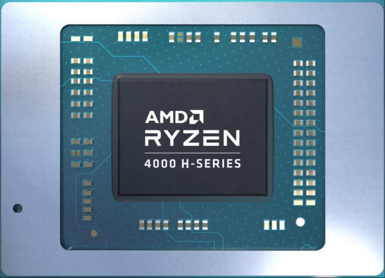
The AMD Ryzen 9 4900HS is a mobile SoC for big laptops based on the Renoir architecture. The 4900HS integrates all eight cores based on the Zen 2 microarchitecture. They are clocked at 3 (guaranteed base clock) to 4.3 GHz (Turbo) and support SMT / Hyperthreading (16 threads). The chip is manufactured in the modern 7 nm process at TSMC and partly thanks to it AMD advertises a 2x improved performance per Watt for the Renoir chips
According to our information, the Ryzen 9 4900HS is only slightly faster than the Ryzen 7 4800HS. The CPU is clocked 100 MHz (base and boost) higher, but the gains greatly depend on the cooling and TDP settings. Compared to Intel chips, the i9-9980HK top model should be comparable. That means the Ryzen 9 4900HS should be able to handle all demanding tasks and gaming. Compared to the similar named 45W-version, the Ryzen 9 4900H, the 4900HS is differs in 100 MHz boost and 300 MHz base clock.
In addition to the eight CPU cores, the APU also integrates a Radeon RX Vega 7 integrated graphics card with most likely 7 CUs. The dual channel memory controller supports DDR4-3200 and energy efficient LPDDR4-4266 RAM. Furthermore, 8 MB level 3 cache can be found on the chip. See our hub page on the Renoir Processors for more information.
The TDP of the APU is specified at 35 Watt (default). That means the chip is intended for big and relatively heavy laptops. The Ryzen 7 4900HS is the 35 Watt version of the R9 4900H with a 10 Watt lower TDP.
| Model | Intel Core i5-1034G1 | AMD Ryzen 9 4900HS | ||||||||
| Series | Intel Ice Lake | AMD Renoir (Ryzen 4000 APU) | ||||||||
| Codename | Ice Lake U | Renoir (Zen 2) | ||||||||
| Series: Ice Lake Ice Lake U |
| |||||||||
| Clock | 800 - 3600 MHz | 3000 - 4300 MHz | ||||||||
| L1 Cache | 192 KB | 512 KB | ||||||||
| L2 Cache | 2 MB | 4 MB | ||||||||
| L3 Cache | 6 MB | 8 MB | ||||||||
| Cores / Threads | 4 / 8 | 8 / 16 | ||||||||
| TDP | 15 Watt | 35 Watt | ||||||||
| Technology | 10 nm | 7 nm | ||||||||
| Features | AVX512, DL Boost, Turbo Boost 2.0 | XFR, FMA3, SSE 4.2, AVX2, SMT | ||||||||
| iGPU | Intel UHD Graphics G1 (Ice Lake 32 EU) (300 MHz) | AMD Radeon RX Vega 8 (Ryzen 4000/5000) ( - 1750 MHz) | ||||||||
| Architecture | x86 | x86 | ||||||||
| Announced | ||||||||||
| max. Temp. | 105 °C | |||||||||
| Socket | FP6 |

