NVIDIA GeForce MX230 vs Intel Iris Plus Graphics G7 (Ice Lake 64 EU) vs NVIDIA GeForce MX250
NVIDIA GeForce MX230 ► remove from comparison
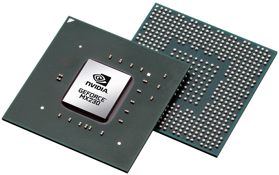
The Nvidia GeForce MX230 is an entry-level dedicated laptop graphics card with DirectX 12 support (FL 12_1) based (most likely) on the Pascal architecture (and not Maxwell as the older MX130). Similar to the faster MX250 , the MX230 is based on the GP108 chip.
Features
The GP108 chip is manufactured in a 14 nm FinFET process at Samsung (LPP) and offers a number of new features, including support for DisplayPort 1.4 (ready), HDMI 2.0b, HDR and improved H.265 video de- and encoding (PlayReady 3.0). 4K HDR with Netflix, however, wont run due to the minimum 3 GB graphics memory that is required. Compared to the bigger Pascal chips, the small GP108 does not support Simultaneous Multi-Projection (SMP) for VR and G-Sync. A full list of improvements and the new Pascal desktop GPUs is available in our dedicated Pascal architecture article
Performance
Thanks to the newer Pascal architecture, the MX230 is significantly faster than the old GeForce MX130 (Maxwell based). Demanding games of 2019 run only in lowest resolution and detail settings and may stutter (e.g. Anno 1800 or Rage 2 ran with under 30fps in our benchmarks). Less demanding games like Overwatch, Fifa 19 or Rocket League, however, can be played in higher detail and resolution settings without stuttering (see benchmarks below).
Power Consumption
The MX230 is manufactured in 14nm at Samsung and due to the low shader count and 64 Bit memory bus, the power consumption is rather low. Therefore, the chip can be also used for small and thin laptops. In our power tests, the faster MX250 needed 22% more power (Furmark load) and the old MX130 even 38% more. The integrated UHD Graphics 620 needed on average only 17% less power at a much lower performance.
Intel Iris Plus Graphics G7 (Ice Lake 64 EU) ► remove from comparison
The Intel Iris Plus Graphics G7 (Ice Lake with 64 EUs) is an integrated graphics card in the Ice Lake SoCs (10th generation core 10xxG7) for laptops. It offers no dedicated graphics memory (no eDRAM cache like the Intel Iris Graphics 655 predecessor of the Coffee Lake SoCs). The clock rate depends on the processor model. At launch it looks like all models have a 300 MHz base clock and only differ in the boost clock (1050 - 1100 MHz). Another difference is the TDP as it can be configured from 12 - 25 Watt in the 15 Watt U-models and maybe even higher in the 25 Watt models that will come later.
The performance should be slightly above a AMD Radeon RX Vega 10 integrated GPU in the Ryzen 7 3000 series processors. e.g. Intel showed a Intel Iris Plus G7 against a Ryzen 7 3700U both configured at 25 Watt TDP and the Ice Lake GPU was able to beat the Vega 10 slightly in all games. Compared to the previous generation, Intel talks about a 2x performance improvement but wont specify the exact model. All in all the GPU should be positioned in the entry level of dedicated GPUs (Nvidia GeForce MX150 level?) and therefore most suited for less demanding games like Fortnite, Rainbow 6 Siege, or Rocket League at reduced details. The theoretical performance of the Chip is specified with 1.12 TFLOPS (FP32) and 2.25 TFLOPS (FP16) when running at 1.1 GHz.
Compared to the older Gen.9 graphics (e.g., UHD Graphics 620 in Whiskey Lake ), Gen.11 is using a wider architecture and also has 3 MB dedicated L3 cache near the GPU.
A special new feature of the Gen11 graphics card is the new Variable Rate Shading (VRS) support. With it game designers can decide where to spend shading time and e.g. shade object in the background or behind fog with less resolution (up to using only one source for a 4x4 block). With this technique early results show up to 1.3x performance in Unreal Engine POC and 1.2x speedup in Civ 6. Up to now VRS is only supported by the new Nvidia Turing architecture (GTX 1650 and up).
Another improved hardware piece is the integrated video de- and encoder that was improved significantly according to Intel. They did not specify any more details, but the previous generation was able to decode VP9 and H.265/HEVC in Main10 profile with 10 bit color depth using the dedicated hardware.
The Iris Plus G7 supports three display pipes that can each output 5K60 signals (via DisplayPort 1.4 HBR3 or HDMI 2.0b). Combining two pipes, the chip is capable to output 8k content.
The Ice Lake SoCs and therefore the integrated GPU are manufactured in the modern 10nm process at Intel that should be comparable to the 7nm process of TSMC.
NVIDIA GeForce MX250 ► remove from comparison
The Nvidia GeForce MX250 is a dedicated entry-level mobile graphics card for laptops . It is based on the same Pascal GP108 chip as the predecessor, the GeForce MX150 / desktop GeForce GT 1030 but features increased clock speeds. As with the MX150, the MX250 is available in two versions, the normal 25 Watt version (1D13 device ID) and a low power version with 10 Watt TDP (1D25 device ID) and reduced performance (The MX150 with 10W had a 32% lower clock speed). The GDDR5 memory interface now also supports speeds up to 3.5 GHz = 7 GHz effective (up from 3 GHz).
The GP108 chip is manufactured in a 14 nm FinFET process at Samsung (LPP) and offers a number of new features, including support for DisplayPort 1.4 (ready), HDMI 2.0b, HDR and improved H.265 video de- and encoding (PlayReady 3.0). 4K HDR with Netflix however wont run due to the minimum 3 GB graphics memory that is required. Compared to the bigger Pascal chips, the small GP108 does not support Simultaneous Multi-Projection (SMP) for VR and G-Sync. A full list of improvements and the new Pascal desktop GPUs is available in our dedicated Pascal architecture article .
Thanks to the increased core speeds (up to +3% in Boost for the 25 Watt version, and faster memory speeds), the new MX250 should be slightly faster than the older MX150. First benchmarks indicate a 5% increase. Still modern should only run fluent in low settings (see the page of the MX150 for games and benchmarks ).
NVIDIA GeForce MX230 Intel Iris Plus Graphics G7 (Ice Lake 64 EU) NVIDIA GeForce MX250 GeForce MX200 Series GeForce MX250 384 @ 1.52 - 1.58 GHz 64 Bit @ 7000 MHz GeForce MX230 256 @ 1.52 - 1.53 GHz 64 Bit @ 7000 MHz
GeForce MX250 384 @ 1.52 - 1.58 GHz 64 Bit @ 7000 MHz GeForce MX230 256 @ 1.52 - 1.53 GHz 64 Bit @ 7000 MHz
Codename N17S-G0 Ice Lake G7 Gen. 11 N17S-G2 Architecture Pascal Gen. 11 Ice Lake Pascal Pipelines 256 - unified 64 - unified 384 - unified Core Speed 1519 - 1531 (Boost) MHz 300 - 1100 (Boost) MHz 1518 - 1582 (Boost) MHz Memory Speed 7000 MHz 7000 effective = 1502 MHz Memory Bus Width 64 Bit 64 Bit Memory Type GDDR5 DDR4 GDDR5 Max. Amount of Memory 4 GB 4 GB Shared Memory no yes no API DirectX 12_1, Shader 5.0, OpenGL 4.5 DirectX 12_1, OpenGL 4.5 DirectX 12_1, OpenGL 4.5 Transistors 1.8 Billion technology 14 nm 10 nm 14 nm Features Vulcan 1.1, GPU Boost 3.0, Optimus, PhysX, CUDA, GeForce Experience, GameWorks QuickSync Vulkan 1.1, OpenGL 4.6, OpenCL 1.2, GPU Boost 3.0, Multi Monitor, Nvidia Optimus Notebook Size medium sized Date of Announcement 20.02.2019 28.05.2019 20.02.2019 Link to Manufacturer Page www.geforce.com www.geforce.com Power Consumption 12-25 Watt 10/25 Watt TMUs 32 ROPs 16 Memory Bandwidth 48.1 GB/s PCIe 3.0
Benchmarks Performance Rating - 3DMark 11 + Fire Strike + Time Spy - GeForce MX230
1.1 pt (3%)
...
...
max:
Performance Rating - 3DMark 11 + Fire Strike + Time Spy - Iris Plus Graphics G7 (Ice Lake 64 EU)
1.3 pt (4%)
...
Intel Iris Plus Graphics G7 (Ice Lake 64 EU)
...
max:
Performance Rating - 3DMark 11 + Fire Strike + Time Spy - GeForce MX250
1.7 pt (5%)
...
...
max:
3DMark - 3DMark Time Spy Score
min: 786 avg: 851 median: 839.5 (2%) max: 937 Points
min: 587 avg: 840 median: 892 (3%) max: 963 Points
min: 980 avg: 1186 median: 1220.5 (4%) max: 1308 Points
3DMark - 3DMark Time Spy Graphics
min: 698 avg: 758 median: 748 (2%) max: 837 Points
min: 526 avg: 744 median: 791 (2%) max: 851 Points
min: 881 avg: 1070 median: 1103 (3%) max: 1169 Points
3DMark - 3DMark Ice Storm Unlimited Graphics
min: 163728 avg: 178637 median: 183041 (21%) max: 189141 Points
min: 101443 avg: 139526 median: 145594 (17%) max: 152365 Points
min: 100071 avg: 213047 median: 235421 (27%) max: 252549 Points
3DMark - 3DMark Ice Storm Extreme Graphics
min: 35141 avg: 61903 median: 74932 (10%) max: 75636 Points
min: 13522 avg: 55230 median: 57777 (7%) max: 68277 Points
min: 22385 avg: 68911 median: 78819 (10%) max: 81895 Points
3DMark - 3DMark Cloud Gate Score
min: 8886 avg: 10432 median: 10529.5 (11%) max: 11659 Points
min: 6616 avg: 12054 median: 12848.5 (14%) max: 14796 Points
min: 8009 avg: 13380 median: 13121 (14%) max: 17955 Points
3DMark - 3DMark Cloud Gate Graphics
min: 13376 avg: 15921 median: 15796.5 (4%) max: 17999 Points
min: 7024 avg: 15496 median: 16713 (4%) max: 18881 Points
min: 13805 avg: 21491 median: 21545 (6%) max: 23863 Points
3DMark - 3DMark Fire Strike Standard Score
min: 2041 avg: 2300 median: 2298.5 (4%) max: 2531 Points
min: 1298 avg: 2400 median: 2559.5 (5%) max: 2925 Points
min: 2726 avg: 3201 median: 3244.5 (6%) max: 3567 Points
3DMark - 3DMark Fire Strike Standard Graphics
min: 2168 avg: 2479 median: 2467.5 (3%) max: 2755 Points
min: 1418 avg: 2594 median: 2743 (3%) max: 3156 Points
min: 2939 avg: 3531 median: 3660 (4%) max: 3885 Points
3DMark - 3DMark Ice Storm Graphics
min: 49120 avg: 78716 median: 84971 (10%) max: 95803 Points
min: 13797 avg: 71013 median: 74928.5 (9%) max: 88374 Points
min: 42088 avg: 80269 median: 86686 (10%) max: 101192 Points
3DMark - 3DMark Wild Life Unlimited
7949 Points (4%)
3DMark - 3DMark Night Raid
min: 7352 avg: 8160 median: 8210.5 (8%) max: 8868 Points
3DMark - 3DMark Night Raid Graphics Score
min: 8615 avg: 9308 median: 9230 (4%) max: 10157 Points
3DMark 11 - 3DM11 Performance Score
min: 3316 avg: 3590 median: 3621.5 (5%) max: 3720 Points
min: 2137 avg: 4186 median: 4436 (6%) max: 4958 Points
min: 3930 avg: 4666 median: 4850 (7%) max: 5302 Points
3DMark 11 - 3DM11 Performance GPU
min: 3180 avg: 3392 median: 3363.5 (3%) max: 3582 Points
min: 2112 avg: 3996 median: 4187 (4%) max: 4630 Points
min: 3585 avg: 4404 median: 4633 (4%) max: 4942 Points
3DMark Vantage + Intel Iris Plus Graphics G7 (Ice Lake 64 EU) 3DMark Vantage - 3DM Vant. Perf. total
14442 Points (4%)
3DM Vant. Perf. total + NVIDIA GeForce MX250
min: 16135 avg: 16488 median: 16487.5 (5%) max: 16840 Points
3DM Vant. Perf. GPU no PhysX + Intel Iris Plus Graphics G7 (Ice Lake 64 EU) 3DMark Vantage - 3DM Vant. Perf. GPU no PhysX
12715 Points (7%)
3DM Vant. Perf. GPU no PhysX + NVIDIA GeForce MX250
min: 15626 avg: 15925 median: 15924.5 (9%) max: 16223 Points
3DMark 03 - 3DMark 03 - Standard
56769 Points (30%)
3DMark 06 3DMark 06 - Standard 1280x1024 + NVIDIA GeForce MX230
18399 Points (24%)
Model CPU GPU RAM Value 3DMark 06 - Standard 1280x1024 Asus VivoBook 14 F412FJ-EB119T (3DMark 06 - Standard 1280x1024) i5-8265U GeForce MX230 2 GB 18399
3DMark 06 - Standard 1280x1024 + Intel Iris Plus Graphics G7 (Ice Lake 64 EU)
min: 8821 avg: 14725 median: 16163.5 (21%) max: 17752 Points
3DMark 06 - Standard 1280x1024 + NVIDIA GeForce MX250
min: 22246 avg: 25429 median: 25428.5 (33%) max: 28611 Points
Unigine Valley 1.0 - Unigine Valley 1.0 DX
17 fps (6%)
Unigine Heaven 3.0 - Unigine Heaven 3.0 DX 11
43.6 fps (14%)
Unigine Heaven 3.0 - Unigine Heaven 3.0 OpenGL
43.7 fps (19%)
Unigine Heaven 2.1 - Heaven 2.1 high
58.9 fps (11%)
SPECviewperf 12 + NVIDIA GeForce MX250 SPECviewperf 12 - specvp12 sw-03
16.7 fps (4%)
specvp12 snx-02 + NVIDIA GeForce MX250 SPECviewperf 12 - specvp12 snx-02
2.1 fps (0%)
specvp12 showcase-01 + NVIDIA GeForce MX250 SPECviewperf 12 - specvp12 showcase-01
16.7 fps (4%)
specvp12 mediacal-01 + NVIDIA GeForce MX250 SPECviewperf 12 - specvp12 mediacal-01
18.1 fps (5%)
specvp12 maya-04 + NVIDIA GeForce MX250 SPECviewperf 12 - specvp12 maya-04
3 fps (1%)
specvp12 energy-01 + NVIDIA GeForce MX250 SPECviewperf 12 - specvp12 energy-01
1.1 fps (1%)
specvp12 creo-01 + NVIDIA GeForce MX250 SPECviewperf 12 - specvp12 creo-01
10.6 fps (4%)
specvp12 catia-04 + NVIDIA GeForce MX250 SPECviewperf 12 - specvp12 catia-04
9.2 fps (2%)
specvp12 3dsmax-05 + NVIDIA GeForce MX250 SPECviewperf 12 - specvp12 3dsmax-05
27.9 fps (5%)
SPECviewperf 13 specvp13 sw-04 + Intel Iris Plus Graphics G7 (Ice Lake 64 EU) SPECviewperf 13 - specvp13 sw-04
7.1 fps (2%)
specvp13 sw-04 + NVIDIA GeForce MX250
34.8 fps (9%)
specvp13 snx-03 + Intel Iris Plus Graphics G7 (Ice Lake 64 EU) SPECviewperf 13 - specvp13 snx-03
2.8 fps (0%)
specvp13 snx-03 + NVIDIA GeForce MX250
6.1 fps (1%)
specvp13 showcase-02 + Intel Iris Plus Graphics G7 (Ice Lake 64 EU) SPECviewperf 13 - specvp13 showcase-02
9.9 fps (2%)
specvp13 showcase-02 + NVIDIA GeForce MX250
16.7 fps (4%)
specvp13 medical-02 + Intel Iris Plus Graphics G7 (Ice Lake 64 EU) SPECviewperf 13 - specvp13 medical-02
4.3 fps (1%)
specvp13 medical-02 + NVIDIA GeForce MX250
10.9 fps (2%)
specvp13 maya-05 + Intel Iris Plus Graphics G7 (Ice Lake 64 EU) SPECviewperf 13 - specvp13 maya-05
20 fps (2%)
specvp13 maya-05 + NVIDIA GeForce MX250
49.5 fps (6%)
specvp13 energy-02 + Intel Iris Plus Graphics G7 (Ice Lake 64 EU) SPECviewperf 13 - specvp13 energy-02
3.5 fps (1%)
specvp13 energy-02 + NVIDIA GeForce MX250 0.5 fps (0%)
specvp13 creo-02 + Intel Iris Plus Graphics G7 (Ice Lake 64 EU) SPECviewperf 13 - specvp13 creo-02
1.7 fps (0%)
specvp13 creo-02 + NVIDIA GeForce MX250
26.7 fps (4%)
specvp13 catia-05 + Intel Iris Plus Graphics G7 (Ice Lake 64 EU) SPECviewperf 13 - specvp13 catia-05
25 fps (3%)
specvp13 catia-05 + NVIDIA GeForce MX250
26.3 fps (3%)
specvp13 3dsmax-06 + Intel Iris Plus Graphics G7 (Ice Lake 64 EU) SPECviewperf 13 - specvp13 3dsmax-06
18.6 fps (3%)
specvp13 3dsmax-06 + NVIDIA GeForce MX250
27.7 fps (5%)
Cinebench R10 Cinebench R10 Shading (32bit) + NVIDIA GeForce MX230 Cinebench R10 - Cinebench R10 Shading (32bit)
min: 4095 avg: 5887 median: 6353 (5%) max: 6748 Points
Cinebench R10 Shading (32bit) + Intel Iris Plus Graphics G7 (Ice Lake 64 EU)
min: 8356 avg: 10332 median: 10554 (7%) max: 11797 Points
Cinebench R10 Shading (32bit) + NVIDIA GeForce MX250
min: 3683 avg: 5523 median: 6469 (5%) max: 6839 Points
Cinebench R11.5 Cinebench R11.5 OpenGL 64 Bit + NVIDIA GeForce MX230 Cinebench R11.5 - Cinebench R11.5 OpenGL 64 Bit
64.7 fps (22%)
Cinebench R11.5 OpenGL 64 Bit + Intel Iris Plus Graphics G7 (Ice Lake 64 EU)
min: 34.72 avg: 45.2 median: 43.8 (15%) max: 52.5 fps
Cinebench R11.5 OpenGL 64 Bit + NVIDIA GeForce MX250
min: 65.6 avg: 73.5 median: 69.6 (24%) max: 85.2 fps
Cinebench R15 + NVIDIA GeForce MX230 Cinebench R15 - Cinebench R15 OpenGL 64 Bit
min: 79.7 avg: 84.3 median: 83.4 (5%) max: 92.5 fps
Cinebench R15 OpenGL 64 Bit + Intel Iris Plus Graphics G7 (Ice Lake 64 EU)
min: 38.4 avg: 62.8 median: 65.2 (4%) max: 74.5 fps
Cinebench R15 OpenGL 64 Bit + NVIDIA GeForce MX250
min: 48.5 avg: 96.8 median: 99.6 (6%) max: 114.8 fps
Cinebench R15 OpenGL Ref. Match 64 Bit + NVIDIA GeForce MX230 Cinebench R15 - Cinebench R15 OpenGL Ref. Match 64 Bit
99.6 % (100%)
Cinebench R15 OpenGL Ref. Match 64 Bit + Intel Iris Plus Graphics G7 (Ice Lake 64 EU)
min: 97.8 avg: 97.9 median: 97.8 (98%) max: 99.3 %
Cinebench R15 OpenGL Ref. Match 64 Bit + NVIDIA GeForce MX250
min: 99.6 avg: 99.6 median: 99.6 (100%) max: 100 %
GFXBench - GFXBench 5.0 Aztec Ruins High Tier Offscreen
9.3 fps (2%)
33.3 fps (6%)
GFXBench - GFXBench 5.0 Aztec Ruins Normal Tier Offscreen
23.5 fps (2%)
79 fps (6%)
GFXBench - GFXBench Car Chase Offscreen
45 fps (5%)
min: 17.6 avg: 41.3 median: 41.3 (5%) max: 64.9 fps
min: 66 avg: 69.5 median: 69.5 (8%) max: 73 fps
GFXBench 3.1 - GFXBench Manhattan ES 3.1 Offscreen
65 fps (1%)
min: 31.2 avg: 59.9 median: 59.9 (1%) max: 88.5 fps
min: 101 avg: 105.3 median: 105.3 (2%) max: 109.6 fps
GFXBench 3.0 - GFXBench 3.0 Manhattan Offscreen
91 fps (5%)
46.6 fps (3%)
min: 136 avg: 141.2 median: 141.2 (8%) max: 146.4 fps
GFXBench (DX / GLBenchmark) 2.7 + NVIDIA GeForce MX230 GFXBench (DX / GLBenchmark) 2.7 - GFXBench T-Rex HD Offscreen C24Z16
176 fps (1%)
GFXBench T-Rex HD Offscreen C24Z16 + Intel Iris Plus Graphics G7 (Ice Lake 64 EU)
min: 84.8 avg: 165.6 median: 165.6 (1%) max: 246.3 fps
GFXBench T-Rex HD Offscreen C24Z16 + NVIDIA GeForce MX250
min: 265 avg: 268.6 median: 268.6 (2%) max: 272.2 fps
Basemark GPU 1.2 - Basemark GPU 1.2 Vulkan Official Medium Offscreen 1080
102 fps (1%)
LuxMark v2.0 64Bit - LuxMark v2.0 Room GPU
583 Samples/s (3%)
min: 224 avg: 392.3 median: 392 (2%) max: 561 Samples/s
min: 505 avg: 629 median: 629 (3%) max: 753 Samples/s
LuxMark v2.0 64Bit - LuxMark v2.0 Sala GPU
1069 Samples/s (2%)
min: 670 avg: 1156 median: 1321 (2%) max: 1478 Samples/s
min: 895 avg: 1173 median: 1172.5 (2%) max: 1450 Samples/s
ComputeMark v2.1 - ComputeMark v2.1 Result
2018 Points (2%)
min: 1527 avg: 2348 median: 2532 (3%) max: 2708 Points
min: 2804 avg: 2806 median: 2806 (3%) max: 2808 Points
Power Consumption - Furmark Stress Test Power Consumption - external Monitor *
33.8 Watt (5%)
min: 17.7 avg: 28.6 median: 28 (4%) max: 39.4 Watt
min: 37.4 avg: 43.3 median: 41.3 (6%) max: 49 Watt
Power Consumption - The Witcher 3 Power Consumption - external Monitor *
min: 18.5 avg: 30.2 median: 30 (4%) max: 42.3 Watt
min: 36 avg: 42.5 median: 43 (6%) max: 48 Watt
Power Consumption - Witcher 3 Power Consumption *
min: 24.5 avg: 37.8 median: 40.4 (9%) max: 48.2 Watt
min: 34.7 avg: 49.9 median: 51 (11%) max: 59.4 Watt
Power Consumption - Witcher 3 ultra Power Efficiency
min: 0.146 avg: 0.2 median: 0.2 (22%) max: 0.2813 fps per Watt
min: 0.1851 avg: 0.2 median: 0.2 (22%) max: 0.2968 fps per Watt
Power Consumption - Witcher 3 ultra Power Efficiency - external Monitor
min: 0.2222 avg: 0.3 median: 0.3 (23%) max: 0.2806 fps per Watt
min: 0.25 avg: 0.3 median: 0.3 (23%) max: 0.2917 fps per Watt
Emissions Witcher 3 Fan Noise + Intel Iris Plus Graphics G7 (Ice Lake 64 EU) Emissions - Witcher 3 Fan Noise
min: 33.4 avg: 38.4 median: 39.2 (63%) max: 43.4 dB(A)
Witcher 3 Fan Noise + NVIDIA GeForce MX250
min: 33.5 avg: 39.3 median: 39.1 (63%) max: 47 dB(A)
Clock Speed - GPU Clock Witcher 3 ultra
min: 463 avg: 616 median: 616 (24%) max: 769 MHz
min: 1481 avg: 1586 median: 1579 (62%) max: 1683 MHz
Clock Speed - GPU Clock Speed Furmark
1300 MHz (52%)
min: 520 avg: 860 median: 820 (32%) max: 1274 MHz
min: 549 avg: 1038 median: 1200 (48%) max: 1571 MHz
Average Benchmarks NVIDIA GeForce MX230 → 100% n=24 Average Benchmarks Intel Iris Plus Graphics G7 (Ice Lake 64 EU) → 98% n=24 Average Benchmarks NVIDIA GeForce MX250 → 129% n=24
- Range of benchmark values for this graphics card
- Average benchmark values for this graphics card
* Smaller numbers mean a higher performance
1 This benchmark is not used for the average calculation
Game Benchmarks The following benchmarks stem from our benchmarks of review laptops. The performance depends on the used graphics memory, clock rate, processor, system settings, drivers, and operating systems. So the results don't have to be representative for all laptops with this GPU. For detailed information on the benchmark results, click on the fps number.
Iris Plus Graphics G7 (Ice Lake 64 EU):
19.8 [X] Lenovo Yoga Slim 7 14IIL05 82A1003NGE Intel Core i7-1065G7 1.3GHz
Iris Plus Graphics G7 (Ice Lake 64 EU)
min:
5.97 fps, P0.1:
8.65 fps, P1:
12.5 fps, max:
30.5 fps
fps
GeForce MX250:
34.8 [X] Lenovo Ideapad S540-14IML Intel Core i7-10510U 1.8GHz
GeForce MX250
min:
11.5 fps, P0.1:
12.8 fps, P1:
18.4 fps, max:
71.3 fps
fps
Iris Plus Graphics G7 (Ice Lake 64 EU):
16.9 [X] Lenovo Yoga Slim 7 14IIL05 82A1003NGE Intel Core i7-1065G7 1.3GHz
Iris Plus Graphics G7 (Ice Lake 64 EU)
min:
4.18 fps, P0.1:
4.83 fps, P1:
9.35 fps, max:
30.4 fps
fps
GeForce MX250:
27.8 [X] Lenovo Ideapad S540-14IML Intel Core i7-10510U 1.8GHz
GeForce MX250
min:
2.79 fps, P0.1:
8.11 fps, P1:
13.6 fps, max:
117.9 fps
fps
GeForce MX250:
26.5 [X] Lenovo Ideapad S540-14IML Intel Core i7-10510U 1.8GHz
GeForce MX250
min:
12.3 fps, P0.1:
13.9 fps, P1:
16.8 fps, max:
47.5 fps
fps
GeForce MX250:
14.4 [X] Lenovo Ideapad S540-14IML Intel Core i7-10510U 1.8GHz
GeForce MX250
min:
9.52 fps, P0.1:
9.55 fps, P1:
10.5 fps, max:
26.7 fps
fps
GeForce MX250:
31 [X] Lenovo Ideapad S540-14IML Intel Core i7-10510U 1.8GHz
GeForce MX250
min:
8.07 fps, P0.1:
17.2 fps, P1:
22 fps, max:
61.1 fps
fps
GeForce MX250:
21.8 [X] Lenovo Ideapad S540-14IML Intel Core i7-10510U 1.8GHz
GeForce MX250
min:
7.38 fps, P0.1:
10.7 fps, P1:
15.7 fps, max:
53.9 fps
fps
GeForce MX250:
18.5 [X] Lenovo Ideapad S540-14IML Intel Core i7-10510U 1.8GHz
GeForce MX250
min:
12.7 fps, P0.1:
12.9 fps, P1:
13.5 fps, max:
38.5 fps
fps
GeForce MX250:
11 [X] Lenovo Ideapad S540-14IML Intel Core i7-10510U 1.8GHz
GeForce MX250
min:
7.97 fps, P0.1:
7.99 fps, P1:
8.14 fps, max:
16.1 fps
fps
GeForce MX250:
3.1 [X] Lenovo Ideapad S540-14IML Intel Core i7-10510U 1.8GHz
GeForce MX250
min:
1 fps, max:
5 fps
fps
Iris Plus Graphics G7 (Ice Lake 64 EU):
12.4 [X] Lenovo Yoga Slim 7 14IIL05 82A1003NGE Intel Core i7-1065G7 1.3GHz
Iris Plus Graphics G7 (Ice Lake 64 EU)
min:
6.12 fps, P0.1:
6.15 fps, P1:
6.34 fps, max:
116.5 fps
fps
GeForce MX250:
10.6 (!) [X] Lenovo Ideapad S540-14IML Intel Core i7-10510U 1.8GHz
GeForce MX250
min:
3.3 fps, P0.1:
3.63 fps, P1:
5.02 fps, max:
135.5 fps
fps
Iris Plus Graphics G7 (Ice Lake 64 EU):
39 [X] Lenovo Yoga Slim 7 14IIL05 82A1003NGE Intel Core i7-1065G7 1.3GHz
Iris Plus Graphics G7 (Ice Lake 64 EU)
fps
GeForce MX250:
45.6 [X] Lenovo Ideapad S540-14IML Intel Core i7-10510U 1.8GHz
GeForce MX250
fps
Iris Plus Graphics G7 (Ice Lake 64 EU):
25 [X] Lenovo Yoga Slim 7 14IIL05 82A1003NGE Intel Core i7-1065G7 1.3GHz
Iris Plus Graphics G7 (Ice Lake 64 EU)
fps
GeForce MX250:
28.2 [X] Lenovo Ideapad S540-14IML Intel Core i7-10510U 1.8GHz
GeForce MX250
fps
Iris Plus Graphics G7 (Ice Lake 64 EU):
13 [X] Lenovo Yoga Slim 7 14IIL05 82A1003NGE Intel Core i7-1065G7 1.3GHz
Iris Plus Graphics G7 (Ice Lake 64 EU)
fps
GeForce MX250:
16.4 [X] Lenovo Ideapad S540-14IML Intel Core i7-10510U 1.8GHz
GeForce MX250
fps
GeForce MX250:
15 [X] Lenovo Ideapad S540-14IML Intel Core i7-10510U 1.8GHz
GeForce MX250
min:
8 fps, max:
64 fps
fps
Iris Plus Graphics G7 (Ice Lake 64 EU):
23.9 [X] Lenovo Yoga Slim 7 14IIL05 82A1003NGE Intel Core i7-1065G7 1.3GHz
Iris Plus Graphics G7 (Ice Lake 64 EU)
min:
19.1 fps, P0.1:
19.8 fps, P1:
21 fps, max:
28.7 fps
fps
GeForce MX250:
22.9 [X] Lenovo Ideapad S540-14IML Intel Core i7-10510U 1.8GHz
GeForce MX250
min:
4.86 fps, P0.1:
6.68 fps, P1:
11.5 fps, max:
128.3 fps
fps
Iris Plus Graphics G7 (Ice Lake 64 EU):
32.1 [X] Lenovo Yoga Slim 7 14IIL05 82A1003NGE Intel Core i7-1065G7 1.3GHz
Iris Plus Graphics G7 (Ice Lake 64 EU)
min:
15.8 fps, P0.1:
16 fps, P1:
17.5 fps, max:
68.4 fps
fps
GeForce MX250:
75.1 [X] Lenovo Ideapad S540-14IML Intel Core i7-10510U 1.8GHz
GeForce MX250
min:
4.71 fps, P0.1:
12 fps, P1:
37.3 fps, max:
299 fps
fps
Iris Plus Graphics G7 (Ice Lake 64 EU):
27.7 [X] Lenovo Yoga Slim 7 14IIL05 82A1003NGE Intel Core i7-1065G7 1.3GHz
Iris Plus Graphics G7 (Ice Lake 64 EU)
min:
1.178 fps, P0.1:
1.767 fps, P1:
11.9 fps, max:
61.5 fps
fps
GeForce MX250:
41 [X] Lenovo Ideapad S540-14IML Intel Core i7-10510U 1.8GHz
GeForce MX250
min:
16.7 fps, P0.1:
18.1 fps, P1:
23.1 fps, max:
90.6 fps
fps
Iris Plus Graphics G7 (Ice Lake 64 EU):
12.8 [X] Lenovo Yoga Slim 7 14IIL05 82A1003NGE Intel Core i7-1065G7 1.3GHz
Iris Plus Graphics G7 (Ice Lake 64 EU)
min:
8.65 fps, P0.1:
8.69 fps, P1:
9.12 fps, max:
19.2 fps
fps
GeForce MX250:
24.3 [X] Lenovo Ideapad S540-14IML Intel Core i7-10510U 1.8GHz
GeForce MX250
min:
11.1 fps, P0.1:
11.4 fps, P1:
14.6 fps, max:
86.3 fps
fps
GeForce MX250:
17.2 [X] Lenovo Ideapad S540-14IML Intel Core i7-10510U 1.8GHz
GeForce MX250
min:
3.47 fps, P0.1:
4.33 fps, P1:
13.4 fps, max:
26.2 fps
fps
Iris Plus Graphics G7 (Ice Lake 64 EU):
10.3 [X] Lenovo Yoga Slim 7 14IIL05 82A1003NGE 2.02
Intel Core i7-1065G7 1.3GHz
Iris Plus Graphics G7 (Ice Lake 64 EU)
min:
7.45 fps, max:
13.7 fps
fps
GeForce MX250:
11.9 [X] Lenovo Ideapad S540-14IML 2.02
Intel Core i7-10510U 1.8GHz
GeForce MX250
min:
5.61 fps, max:
23.2 fps
fps
GeForce MX250:
9 [X] Lenovo Ideapad S540-14IML 2.02
Intel Core i7-10510U 1.8GHz
GeForce MX250
min:
5.31 fps, max:
14.5 fps
fps
GeForce MX250:
5 [X] Lenovo Ideapad S540-14IML 2.02
Intel Core i7-10510U 1.8GHz
GeForce MX250
min:
3.12 fps, max:
8.13 fps
fps
GeForce MX250:
4.2 [X] Lenovo Ideapad S540-14IML 2.02
Intel Core i7-10510U 1.8GHz
GeForce MX250
min:
2.81 fps, max:
7.26 fps
fps
Iris Plus Graphics G7 (Ice Lake 64 EU):
12.7 [X] Lenovo Yoga Slim 7 14IIL05 82A1003NGE Intel Core i7-1065G7 1.3GHz
Iris Plus Graphics G7 (Ice Lake 64 EU)
min:
5.83 fps, P0.1:
5.84 fps, P1:
6.08 fps, max:
125.2 fps
fps
GeForce MX250:
17.7 [X] Lenovo Ideapad S540-14IML Intel Core i7-10510U 1.8GHz
GeForce MX250
min:
7.74 fps, P0.1:
7.76 fps, P1:
8.11 fps, max:
136.9 fps
fps
GeForce MX250:
16.6 [X] Lenovo Ideapad S540-14IML Intel Core i7-10510U 1.8GHz
GeForce MX250
min:
5.6 fps, P0.1:
5.61 fps, P1:
6.05 fps, max:
132.5 fps
fps
GeForce MX250:
16.5 [X] Lenovo Ideapad S540-14IML Intel Core i7-10510U 1.8GHz
GeForce MX250
min:
6.3 fps, P0.1:
6.73 fps, P1:
7.3 fps, max:
124.7 fps
fps
GeForce MX250:
9.5 [X] Lenovo Ideapad S540-14IML Intel Core i7-10510U 1.8GHz
GeForce MX250
min:
4.12 fps, P0.1:
4.16 fps, P1:
4.45 fps, max:
91.4 fps
fps
GeForce MX250:
9.8 [X] Lenovo Ideapad S540-14IML Intel Core i7-10510U 1.8GHz
GeForce MX250
min:
7.1 fps, P0.1:
7.17 fps, P1:
7.55 fps, max:
13.8 fps
fps
Iris Plus Graphics G7 (Ice Lake 64 EU):
14.6 [X] Lenovo Yoga Slim 7 14IIL05 82A1003NGE Intel Core i7-1065G7 1.3GHz
Iris Plus Graphics G7 (Ice Lake 64 EU)
min:
7.37 fps, P0.1:
9.56 fps, P1:
12.6 fps, max:
34.5 fps
fps
GeForce MX250:
13.7 [X] Lenovo Ideapad S540-14IML Intel Core i7-10510U 1.8GHz
GeForce MX250
min:
9.18 fps, P0.1:
9.38 fps, P1:
9.9 fps, max:
47 fps
fps
Iris Plus Graphics G7 (Ice Lake 64 EU):
11.9 [X] Lenovo Yoga Slim 7 14IIL05 82A1003NGE Intel Core i7-1065G7 1.3GHz
Iris Plus Graphics G7 (Ice Lake 64 EU)
min:
6.47 fps, P0.1:
8.04 fps, P1:
10.3 fps, max:
21.8 fps
fps
GeForce MX250:
10.2 [X] Lenovo Ideapad S540-14IML Intel Core i7-10510U 1.8GHz
GeForce MX250
min:
6.44 fps, P0.1:
6.54 fps, P1:
8.09 fps, max:
14.7 fps
fps
GeForce MX250:
4.2 [X] Lenovo Ideapad S540-14IML Intel Core i7-10510U 1.8GHz
GeForce MX250
min:
2.33 fps, P0.1:
2.34 fps, P1:
2.53 fps, max:
6.87 fps
fps
GeForce MX250:
9.1 [X] Lenovo Ideapad S540-14IML Intel Core i7-10510U 1.8GHz
GeForce MX250
min:
4.15 fps, P0.1:
4.26 fps, P1:
4.53 fps, max:
101 fps
fps
GeForce MX250:
15.3 [X] Lenovo Ideapad S540-14IML Intel Core i7-10510U 1.8GHz
GeForce MX250
min:
12.2 fps, P0.1:
12.4 fps, P1:
12.9 fps, max:
21 fps
fps
GeForce MX250:
23.2 [X] Lenovo Ideapad S540-14IML 1057599
Intel Core i7-10510U 1.8GHz
GeForce MX250
min:
17 fps, P1:
16 fps, max:
32 fps
fps
GeForce MX250:
20 [X] Lenovo Ideapad S540-14IML 1057599
Intel Core i7-10510U 1.8GHz
GeForce MX250
min:
15 fps, P1:
15 fps, max:
27 fps
fps
GeForce MX250:
13.7 [X] Lenovo Ideapad S540-14IML 1057599
Intel Core i7-10510U 1.8GHz
GeForce MX250
min:
8 fps, P1:
10 fps, max:
17 fps
fps
GeForce MX250:
8.1 [X] Lenovo Ideapad S540-14IML 1057599
Intel Core i7-10510U 1.8GHz
GeForce MX250
min:
1 fps, P1:
6 fps, max:
10 fps
fps
GeForce MX250:
30.5 [X] Lenovo Ideapad S540-14IML Intel Core i7-10510U 1.8GHz
GeForce MX250
min:
14.4 fps, P0.1:
15.6 fps, P1:
23 fps, max:
95.3 fps
fps
GeForce MX250:
26.5 [X] Lenovo Ideapad S540-14IML Intel Core i7-10510U 1.8GHz
GeForce MX250
min:
5.46 fps, P0.1:
5.59 fps, P1:
15.3 fps, max:
143.2 fps
fps
GeForce MX250:
24.5 [X] Lenovo Ideapad S540-14IML Intel Core i7-10510U 1.8GHz
GeForce MX250
min:
7.24 fps, P0.1:
7.3 fps, P1:
12.4 fps, max:
61.5 fps
fps
GeForce MX250:
22.2 [X] Lenovo Ideapad S540-14IML Intel Core i7-10510U 1.8GHz
GeForce MX250
min:
6.89 fps, P0.1:
8.93 fps, P1:
14.2 fps, max:
85.6 fps
fps
GeForce MX250:
7.4 [X] Lenovo Ideapad S540-14IML Intel Core i7-10510U 1.8GHz
GeForce MX250
min:
3.37 fps, P0.1:
3.7 fps, P1:
5.51 fps, max:
66.5 fps
fps
Iris Plus Graphics G7 (Ice Lake 64 EU):
20.5 [X] Lenovo Yoga Slim 7 14IIL05 82A1003NGE Intel Core i7-1065G7 1.3GHz
Iris Plus Graphics G7 (Ice Lake 64 EU)
min:
5.16 fps, P0.1:
6.82 fps, P1:
11 fps, max:
105.6 fps
fps
GeForce MX250:
32.5 [X] Lenovo Ideapad S540-14IML Intel Core i7-10510U 1.8GHz
GeForce MX250
min:
14.4 fps, P0.1:
14.9 fps, P1:
16.9 fps, max:
157 fps
fps
Iris Plus Graphics G7 (Ice Lake 64 EU):
16.5 [X] Lenovo Yoga Slim 7 14IIL05 82A1003NGE Intel Core i7-1065G7 1.3GHz
Iris Plus Graphics G7 (Ice Lake 64 EU)
min:
2.96 fps, P0.1:
3.05 fps, P1:
3.71 fps, max:
104.8 fps
fps
GeForce MX250:
27.5 [X] Lenovo Ideapad S540-14IML Intel Core i7-10510U 1.8GHz
GeForce MX250
min:
5.33 fps, P0.1:
6 fps, P1:
14.9 fps, max:
92.2 fps
fps
Iris Plus Graphics G7 (Ice Lake 64 EU):
12.4 [X] Lenovo Yoga Slim 7 14IIL05 82A1003NGE Intel Core i7-1065G7 1.3GHz
Iris Plus Graphics G7 (Ice Lake 64 EU)
min:
6.17 fps, P0.1:
6.3 fps, P1:
6.9 fps, max:
65.3 fps
fps
GeForce MX250:
21.1 [X] Lenovo Ideapad S540-14IML Intel Core i7-10510U 1.8GHz
GeForce MX250
min:
7.99 fps, P0.1:
8.58 fps, P1:
12.4 fps, max:
89.2 fps
fps
GeForce MX250:
15.2 [X] Lenovo Ideapad S540-14IML Intel Core i7-10510U 1.8GHz
GeForce MX250
min:
3.89 fps, P0.1:
4.01 fps, P1:
6.43 fps, max:
71.1 fps
fps
GeForce MX250:
12.9 [X] Lenovo Ideapad S540-14IML Intel Core i7-10510U 1.8GHz
GeForce MX250
min:
6.4 fps, P0.1:
6.7 fps, P1:
8.59 fps, max:
21.2 fps
fps
Iris Plus Graphics G7 (Ice Lake 64 EU):
18.6 [X] Lenovo Yoga Slim 7 14IIL05 82A1003NGE Intel Core i7-1065G7 1.3GHz
Iris Plus Graphics G7 (Ice Lake 64 EU)
P0.1:
13.7 fpsP1:
14.4 fps
fps
GeForce MX250:
14.1 [X] Lenovo Ideapad S540-14IML Intel Core i7-10510U 1.8GHz
GeForce MX250
P0.1:
7.4 fpsP1:
10 fps
fps
Iris Plus Graphics G7 (Ice Lake 64 EU):
8.5 [X] Lenovo Yoga Slim 7 14IIL05 82A1003NGE Intel Core i7-1065G7 1.3GHz
Iris Plus Graphics G7 (Ice Lake 64 EU)
min:
2.46 fps, P0.1:
2.46 fps, P1:
2.69 fps, max:
17.1 fps
fps
GeForce MX250:
20 [X] Lenovo Ideapad S540-14IML Intel Core i7-10510U 1.8GHz
GeForce MX250
min:
8.89 fps, P0.1:
9.14 fps, P1:
14.4 fps, max:
48.5 fps
fps
GeForce MX250:
10.7 [X] Lenovo Ideapad S540-14IML Intel Core i7-10510U 1.8GHz
GeForce MX250
min:
4.83 fps, P0.1:
5.5 fps, P1:
7.91 fps, max:
21.5 fps
fps
Iris Plus Graphics G7 (Ice Lake 64 EU):
15.2 [X] Lenovo Yoga Slim 7 14IIL05 82A1003NGE Intel Core i7-1065G7 1.3GHz
Iris Plus Graphics G7 (Ice Lake 64 EU)
min:
13.1 fps, P0.1:
13.1 fps, P1:
13.3 fps, max:
17.3 fps
fps
GeForce MX250:
26.6 [X] Lenovo Ideapad S540-14IML Intel Core i7-10510U 1.8GHz
GeForce MX250
min:
17.7 fps, P0.1:
18.8 fps, P1:
21.7 fps, max:
41.9 fps
fps
Iris Plus Graphics G7 (Ice Lake 64 EU):
11.6 [X] Lenovo Yoga Slim 7 14IIL05 82A1003NGE Intel Core i7-1065G7 1.3GHz
Iris Plus Graphics G7 (Ice Lake 64 EU)
min:
10 fps, P0.1:
10 fps, P1:
10.3 fps, max:
13.2 fps
fps
GeForce MX250:
19.5 [X] Lenovo Ideapad S540-14IML Intel Core i7-10510U 1.8GHz
GeForce MX250
min:
13.1 fps, P0.1:
13.9 fps, P1:
16.1 fps, max:
34.5 fps
fps
GeForce MX250:
7.4 [X] Lenovo Ideapad S540-14IML Intel Core i7-10510U 1.8GHz
GeForce MX250
min:
4.42 fps, P0.1:
5 fps, P1:
6.13 fps, max:
16.8 fps
fps
GeForce MX250:
8 [X] Lenovo Ideapad S540-14IML Intel Core i7-10510U 1.8GHz
GeForce MX250
min:
3 fps, max:
21 fps
fps
Iris Plus Graphics G7 (Ice Lake 64 EU):
11.2 [X] Lenovo Yoga Slim 7 14IIL05 82A1003NGE Intel Core i7-1065G7 1.3GHz
Iris Plus Graphics G7 (Ice Lake 64 EU)
min:
5.85 fps, P0.1:
6.43 fps, P1:
9.03 fps, max:
48.4 fps
fps
GeForce MX250:
14.5 [X] Lenovo Ideapad S540-14IML Intel Core i7-10510U 1.8GHz
GeForce MX250
min:
10.2 fps, P0.1:
10.3 fps, P1:
10.8 fps, max:
23.7 fps
fps
GeForce MX250:
7.7 [X] Lenovo Ideapad S540-14IML Intel Core i7-10510U 1.8GHz
GeForce MX250
min:
2.02 fps, P0.1:
2.08 fps, P1:
2.66 fps, max:
36.6 fps
fps
Iris Plus Graphics G7 (Ice Lake 64 EU):
7.5 (!) [X] Lenovo Yoga Slim 7 14IIL05 82A1003NGE Intel Core i7-1065G7 1.3GHz
Iris Plus Graphics G7 (Ice Lake 64 EU)
min:
5.84 fps, P0.1:
5.88 fps, P1:
6.23 fps, max:
10.4 fps
fps
GeForce MX250:
7.9 [X] Lenovo Ideapad S540-14IML Intel Core i7-10510U 1.8GHz
GeForce MX250
min:
2.59 fps, P0.1:
2.66 fps, P1:
3.12 fps, max:
58.6 fps
fps
GeForce MX250:
28.2 [X] Lenovo Ideapad S540-14IML Intel Core i7-10510U 1.8GHz
GeForce MX250
min:
6.39 fps, P0.1:
10.4 fps, P1:
17.6 fps, max:
124.8 fps
fps
GeForce MX250:
20.7 [X] Lenovo Ideapad S540-14IML Intel Core i7-10510U 1.8GHz
GeForce MX250
min:
6.65 fps, P0.1:
6.66 fps, P1:
12.6 fps, max:
136.8 fps
fps
GeForce MX250:
7.8 [X] Lenovo Ideapad S540-14IML Intel Core i7-10510U 1.8GHz
GeForce MX250
min:
6.34 fps, P0.1:
6.45 fps, P1:
6.84 fps, max:
8.82 fps
fps
Iris Plus Graphics G7 (Ice Lake 64 EU):
24.1 [X] Lenovo Yoga Slim 7 14IIL05 82A1003NGE Intel Core i7-1065G7 1.3GHz
Iris Plus Graphics G7 (Ice Lake 64 EU)
min:
8.51 fps, P0.1:
8.51 fps, P1:
10.2 fps, max:
132.3 fps
fps
GeForce MX250:
24 [X] Lenovo Ideapad S540-14IML Intel Core i7-10510U 1.8GHz
GeForce MX250
min:
10.1 fps, P0.1:
10.2 fps, P1:
10.9 fps, max:
153.2 fps
fps
Iris Plus Graphics G7 (Ice Lake 64 EU):
13.4 [X] Lenovo Yoga Slim 7 14IIL05 82A1003NGE Intel Core i7-1065G7 1.3GHz
Iris Plus Graphics G7 (Ice Lake 64 EU)
min:
4.97 fps, P0.1:
5.05 fps, P1:
5.72 fps, max:
75.7 fps
fps
GeForce MX250:
14.4 [X] Lenovo Ideapad S540-14IML Intel Core i7-10510U 1.8GHz
GeForce MX250
min:
5.71 fps, P0.1:
5.79 fps, P1:
6.24 fps, max:
112.2 fps
fps
Iris Plus Graphics G7 (Ice Lake 64 EU):
12 [X] Lenovo Yoga Slim 7 14IIL05 82A1003NGE Intel Core i7-1065G7 1.3GHz
Iris Plus Graphics G7 (Ice Lake 64 EU)
min:
4.38 fps, P0.1:
4.4 fps, P1:
4.57 fps, max:
85.3 fps
fps
GeForce MX250:
11.6 [X] Lenovo Ideapad S540-14IML Intel Core i7-10510U 1.8GHz
GeForce MX250
min:
5.12 fps, P0.1:
5.13 fps, P1:
5.24 fps, max:
80.1 fps
fps
Iris Plus Graphics G7 (Ice Lake 64 EU):
14.1 [X] Lenovo Yoga Slim 7 14IIL05 82A1003NGE Intel Core i7-1065G7 1.3GHz
Iris Plus Graphics G7 (Ice Lake 64 EU)
fps
GeForce MX250:
23.9 [X] Lenovo Ideapad S540-14IML Intel Core i7-10510U 1.8GHz
GeForce MX250
fps
GeForce MX250:
13.9 [X] Lenovo Ideapad S540-14IML Intel Core i7-10510U 1.8GHz
GeForce MX250
fps
GeForce MX250:
10 [X] Lenovo Ideapad S540-14IML Intel Core i7-10510U 1.8GHz
GeForce MX250
fps
Iris Plus Graphics G7 (Ice Lake 64 EU):
12.8 [X] Lenovo Yoga Slim 7 14IIL05 82A1003NGE Intel Core i7-1065G7 1.3GHz
Iris Plus Graphics G7 (Ice Lake 64 EU)
min:
3.09 fps, P0.1:
6.83 fps, P1:
9.75 fps, max:
171.4 fps
fps
GeForce MX250:
14.4 [X] Lenovo Ideapad S540-14IML Intel Core i7-10510U 1.8GHz
GeForce MX250
min:
4.36 fps, P0.1:
5.28 fps, P1:
11 fps, max:
207 fps
fps
GeForce MX250:
18 [X] Lenovo Ideapad S540-14IML Intel Core i7-10510U 1.8GHz
GeForce MX250
min:
11 fps
fps
GeForce MX250:
15 [X] Lenovo Ideapad S540-14IML Intel Core i7-10510U 1.8GHz
GeForce MX250
min:
9 fps
fps
Iris Plus Graphics G7 (Ice Lake 64 EU):
8.5 [X] Lenovo Yoga Slim 7 14IIL05 82A1003NGE Intel Core i7-1065G7 1.3GHz
Iris Plus Graphics G7 (Ice Lake 64 EU)
min:
7.45 fps, P0.1:
7.47 fps, P1:
7.58 fps, max:
9.73 fps
fps
GeForce MX250:
6 [X] Lenovo Ideapad S540-14IML Intel Core i7-10510U 1.8GHz
GeForce MX250
min:
5.05 fps, P0.1:
5.06 fps, P1:
5.08 fps, max:
6.78 fps
fps
GeForce MX250:
13.1 [X] Lenovo Ideapad S540-14IML Intel Core i7-10510U 1.8GHz
GeForce MX250
min:
7.92 fps, P0.1:
8.08 fps, P1:
8.95 fps, max:
20.4 fps
fps
Iris Plus Graphics G7 (Ice Lake 64 EU):
11 [X] Lenovo Yoga Slim 7 14IIL05 82A1003NGE Intel Core i7-1065G7 1.3GHz
Iris Plus Graphics G7 (Ice Lake 64 EU)
min:
6.21 fps, P0.1:
6.41 fps, P1:
7.61 fps, max:
20.4 fps
fps
GeForce MX250:
19.4 [X] Lenovo Ideapad S540-14IML Intel Core i7-10510U 1.8GHz
GeForce MX250
min:
15 fps, P0.1:
15.2 fps, P1:
16.9 fps, max:
25.3 fps
fps
GeForce MX250:
14.1 [X] Lenovo Ideapad S540-14IML Intel Core i7-10510U 1.8GHz
GeForce MX250
min:
8.93 fps, P0.1:
9.68 fps, P1:
11 fps, max:
21.4 fps
fps
GeForce MX250:
10.4 [X] Lenovo Ideapad S540-14IML Intel Core i7-10510U 1.8GHz
GeForce MX250
min:
5.96 fps, P0.1:
6.21 fps, P1:
7.48 fps, max:
17.6 fps
fps
GeForce MX250:
29.6 [X] Lenovo Ideapad S540-14IML 959964
Intel Core i7-10510U 1.8GHz
GeForce MX250
min:
19 fps, P1:
18 fps, max:
36 fps
fps
GeForce MX250:
28.1 [X] Lenovo Ideapad S540-14IML 959964
Intel Core i7-10510U 1.8GHz
GeForce MX250
min:
23 fps, P1:
21 fps, max:
32 fps
fps
GeForce MX250:
20 [X] Lenovo Ideapad S540-14IML 959964
Intel Core i7-10510U 1.8GHz
GeForce MX250
min:
16 fps, P1:
15 fps, max:
22 fps
fps
GeForce MX250:
11 [X] Lenovo Ideapad S540-14IML 959964
Intel Core i7-10510U 1.8GHz
GeForce MX250
min:
8 fps, P1:
8 fps, max:
13 fps
fps
Iris Plus Graphics G7 (Ice Lake 64 EU):
38.2 [X] Lenovo Yoga Slim 7 14IIL05 82A1003NGE Intel Core i7-1065G7 1.3GHz
Iris Plus Graphics G7 (Ice Lake 64 EU)
min:
25.2 fps, P0.1:
26 fps, P1:
28.5 fps, max:
56.3 fps
fps
GeForce MX250:
37.8 [X] Lenovo Ideapad S540-14IML Intel Core i7-10510U 1.8GHz
GeForce MX250
min:
4.92 fps, P0.1:
7.55 fps, P1:
20.2 fps, max:
79.4 fps
fps
Iris Plus Graphics G7 (Ice Lake 64 EU):
22.6 [X] Lenovo Yoga Slim 7 14IIL05 82A1003NGE Intel Core i7-1065G7 1.3GHz
Iris Plus Graphics G7 (Ice Lake 64 EU)
min:
7.57 fps, P0.1:
8.04 fps, P1:
16.7 fps, max:
83.4 fps
fps
GeForce MX250:
26.8 [X] Lenovo Ideapad S540-14IML Intel Core i7-10510U 1.8GHz
GeForce MX250
min:
4.13 fps, P0.1:
5.91 fps, P1:
14.4 fps, max:
52.2 fps
fps
Iris Plus Graphics G7 (Ice Lake 64 EU):
19.1 [X] Lenovo Yoga Slim 7 14IIL05 82A1003NGE Intel Core i7-1065G7 1.3GHz
Iris Plus Graphics G7 (Ice Lake 64 EU)
min:
13.5 fps, P0.1:
13.6 fps, P1:
14.7 fps, max:
29.1 fps
fps
GeForce MX250:
24.4 [X] Lenovo Ideapad S540-14IML Intel Core i7-10510U 1.8GHz
GeForce MX250
min:
5.95 fps, P0.1:
6.53 fps, P1:
12.5 fps, max:
48.2 fps
fps
Iris Plus Graphics G7 (Ice Lake 64 EU):
16.8 [X] Lenovo Yoga Slim 7 14IIL05 82A1003NGE Intel Core i7-1065G7 1.3GHz
Iris Plus Graphics G7 (Ice Lake 64 EU)
min:
13.1 fps, P0.1:
13.3 fps, P1:
13.8 fps, max:
22 fps
fps
GeForce MX250:
17.6 [X] Lenovo Ideapad S540-14IML Intel Core i7-10510U 1.8GHz
GeForce MX250
min:
5.7 fps, P0.1:
6.45 fps, P1:
8.68 fps, max:
48.6 fps
fps
Iris Plus Graphics G7 (Ice Lake 64 EU):
13.8 [X] Lenovo Yoga Slim 7 14IIL05 82A1003NGE Intel Core i7-1065G7 1.3GHz
Iris Plus Graphics G7 (Ice Lake 64 EU)
min:
4.4 fps, P0.1:
4.97 fps, P1:
7.3 fps, max:
83.7 fps
fps
GeForce MX250:
20.3 [X] Lenovo Ideapad S540-14IML Intel Core i7-10510U 1.8GHz
GeForce MX250
min:
8.97 fps, P0.1:
9.01 fps, P1:
10.1 fps, max:
115 fps
fps
GeForce MX250:
15.5 [X] Lenovo Ideapad S540-14IML Intel Core i7-10510U 1.8GHz
GeForce MX250
min:
6.66 fps, P0.1:
6.88 fps, P1:
7.66 fps, max:
113.9 fps
fps
GeForce MX250:
13.9 [X] Lenovo Ideapad S540-14IML Intel Core i7-10510U 1.8GHz
GeForce MX250
min:
5.78 fps, P0.1:
5.83 fps, P1:
6.64 fps, max:
105.2 fps
fps
GeForce MX250:
13.6 [X] Lenovo Ideapad S540-14IML Intel Core i7-10510U 1.8GHz
GeForce MX250
min:
6.45 fps, P0.1:
6.49 fps, P1:
6.76 fps, max:
116.6 fps
fps
Iris Plus Graphics G7 (Ice Lake 64 EU):
17.7 [X] Lenovo Yoga Slim 7 14IIL05 82A1003NGE Intel Core i7-1065G7 1.3GHz
Iris Plus Graphics G7 (Ice Lake 64 EU)
fps
GeForce MX250:
20.8 [X] Lenovo Ideapad S540-14IML Intel Core i7-10510U 1.8GHz
GeForce MX250
fps
GeForce MX250:
13 [X] Lenovo Ideapad S540-14IML Intel Core i7-10510U 1.8GHz
GeForce MX250
fps
GeForce MX250:
7.2 [X] Lenovo Ideapad S540-14IML Intel Core i7-10510U 1.8GHz
GeForce MX250
fps
GeForce MX250:
14.1 [X] Lenovo Ideapad S540-14IML Intel Core i7-10510U 1.8GHz
GeForce MX250
min:
9.3 fps, max:
21.4 fps
fps
GeForce MX250:
10.6 [X] Lenovo Ideapad S540-14IML Intel Core i7-10510U 1.8GHz
GeForce MX250
min:
4.9 fps, max:
16.2 fps
fps
GeForce MX250:
16.2 [X] Lenovo Ideapad S540-14IML Intel Core i7-10510U 1.8GHz
GeForce MX250
min:
7.92 fps, P0.1:
8.1 fps, P1:
8.52 fps, max:
72.2 fps
fps
GeForce MX250:
43.3 [X] Lenovo Ideapad S540-14IML 549884
Intel Core i7-10510U 1.8GHz
GeForce MX250
min:
10 fps, max:
165.3 fps
fps
GeForce MX250:
26.4 [X] Lenovo Ideapad S540-14IML 549884
Intel Core i7-10510U 1.8GHz
GeForce MX250
min:
6.65 fps, max:
132.8 fps
fps
GeForce MX250:
22.4 [X] Lenovo Ideapad S540-14IML 549884
Intel Core i7-10510U 1.8GHz
GeForce MX250
min:
5.6 fps, max:
124.4 fps
fps
GeForce MX250:
15.3 [X] Lenovo Ideapad S540-14IML 549884
Intel Core i7-10510U 1.8GHz
GeForce MX250
min:
4.14 fps, max:
121.8 fps
fps
Iris Plus Graphics G7 (Ice Lake 64 EU):
15.5 [X] Lenovo Yoga Slim 7 14IIL05 82A1003NGE Intel Core i7-1065G7 1.3GHz
Iris Plus Graphics G7 (Ice Lake 64 EU)
min:
6.9 fps, P0.1:
9.19 fps, P1:
12.4 fps, max:
35.6 fps
fps
GeForce MX250:
21.4 [X] Lenovo Ideapad S540-14IML Intel Core i7-10510U 1.8GHz
GeForce MX250
min:
13.9 fps, P0.1:
14.3 fps, P1:
15.8 fps, max:
38.2 fps
fps
Iris Plus Graphics G7 (Ice Lake 64 EU):
12.7 [X] Lenovo Yoga Slim 7 14IIL05 82A1003NGE Intel Core i7-1065G7 1.3GHz
Iris Plus Graphics G7 (Ice Lake 64 EU)
min:
7.44 fps, P0.1:
8.87 fps, P1:
10.7 fps, max:
19 fps
fps
GeForce MX250:
11.2 [X] Lenovo Ideapad S540-14IML Intel Core i7-10510U 1.8GHz
GeForce MX250
min:
7.95 fps, P0.1:
8.63 fps, P1:
9.18 fps, max:
15.8 fps
fps
GeForce MX250:
12.6 [X] Lenovo Ideapad S540-14IML Intel Core i7-10510U 1.8GHz
GeForce MX250
min:
9.95 fps, P0.1:
10 fps, P1:
11.4 fps, max:
14.9 fps
fps
GeForce MX250:
9.6 [X] Lenovo Ideapad S540-14IML Intel Core i7-10510U 1.8GHz
GeForce MX250
min:
8.95 fps, P0.1:
8.96 fps, P1:
9.02 fps, max:
10.7 fps
fps
Iris Plus Graphics G7 (Ice Lake 64 EU):
23 [X] Lenovo Yoga Slim 7 14IIL05 82A1003NGE Intel Core i7-1065G7 1.3GHz
Iris Plus Graphics G7 (Ice Lake 64 EU)
min:
16 fps, max:
29 fps
fps
GeForce MX250:
28 [X] Lenovo Ideapad S540-14IML Intel Core i7-10510U 1.8GHz
GeForce MX250
min:
13 fps, max:
34 fps
fps
Iris Plus Graphics G7 (Ice Lake 64 EU):
17 [X] Lenovo Yoga Slim 7 14IIL05 82A1003NGE Intel Core i7-1065G7 1.3GHz
Iris Plus Graphics G7 (Ice Lake 64 EU)
min:
11 fps, max:
22 fps
fps
GeForce MX250:
19 [X] Lenovo Ideapad S540-14IML Intel Core i7-10510U 1.8GHz
GeForce MX250
min:
13 fps, max:
24 fps
fps
GeForce MX250:
15 [X] Lenovo Ideapad S540-14IML Intel Core i7-10510U 1.8GHz
GeForce MX250
min:
9 fps, max:
21 fps
fps
GeForce MX250:
14.8 [X] Lenovo Ideapad S540-14IML Intel Core i7-10510U 1.8GHz
GeForce MX250
min:
6.68 fps, P0.1:
7.07 fps, P1:
9.18 fps, max:
17.9 fps
fps
GeForce MX250:
12.5 [X] Lenovo Ideapad S540-14IML Intel Core i7-10510U 1.8GHz
GeForce MX250
min:
4.92 fps, P0.1:
5 fps, P1:
5.24 fps, max:
34.7 fps
fps
GeForce MX250:
5.7 [X] Lenovo Ideapad S540-14IML Intel Core i7-10510U 1.8GHz
GeForce MX250
min:
2.94 fps, P0.1:
3.02 fps, P1:
3.56 fps, max:
7.73 fps
fps
GeForce MX250:
87.4 [X] Lenovo Ideapad S540-14IML Intel Core i7-10510U 1.8GHz
GeForce MX250
min:
11.2 fps, P0.1:
17.3 fps, P1:
61.3 fps, max:
133.7 fps
fps
GeForce MX250:
33 [X] Lenovo Ideapad S540-14IML Intel Core i7-10510U 1.8GHz
GeForce MX250
min:
4.63 fps, P0.1:
5.04 fps, P1:
8.42 fps, max:
113 fps
fps
GeForce MX250:
23.4 [X] Lenovo Ideapad S540-14IML Intel Core i7-10510U 1.8GHz
GeForce MX250
min:
2.49 fps, P0.1:
2.88 fps, P1:
4.58 fps, max:
69.3 fps
fps
Iris Plus Graphics G7 (Ice Lake 64 EU):
28 [X] Lenovo Yoga Slim 7 14IIL05 82A1003NGE Intel Core i7-1065G7 1.3GHz
Iris Plus Graphics G7 (Ice Lake 64 EU)
fps
GeForce MX250:
47 [X] Lenovo Ideapad S540-14IML Intel Core i7-10510U 1.8GHz
GeForce MX250
fps
Iris Plus Graphics G7 (Ice Lake 64 EU):
15 [X] Lenovo Yoga Slim 7 14IIL05 82A1003NGE Intel Core i7-1065G7 1.3GHz
Iris Plus Graphics G7 (Ice Lake 64 EU)
fps
GeForce MX250:
17 [X] Lenovo Ideapad S540-14IML Intel Core i7-10510U 1.8GHz
GeForce MX250
fps
GeForce MX250:
13 [X] Lenovo Ideapad S540-14IML Intel Core i7-10510U 1.8GHz
GeForce MX250
fps
Iris Plus Graphics G7 (Ice Lake 64 EU):
19 [X] Lenovo Yoga Slim 7 14IIL05 82A1003NGE Intel Core i7-1065G7 1.3GHz
Iris Plus Graphics G7 (Ice Lake 64 EU)
min:
9 fps, max:
24 fps
fps
GeForce MX250:
38 [X] Lenovo Ideapad S540-14IML Intel Core i7-10510U 1.8GHz
GeForce MX250
min:
28 fps, max:
55 fps
fps
GeForce MX250:
16 [X] Lenovo Ideapad S540-14IML Intel Core i7-10510U 1.8GHz
GeForce MX250
min:
4 fps, max:
23 fps
fps
GeForce MX250:
12 [X] Lenovo Ideapad S540-14IML Intel Core i7-10510U 1.8GHz
GeForce MX250
min:
9 fps, max:
18 fps
fps
Iris Plus Graphics G7 (Ice Lake 64 EU):
46.6 [X] Lenovo Yoga Slim 7 14IIL05 82A1003NGE Intel Core i7-1065G7 1.3GHz
Iris Plus Graphics G7 (Ice Lake 64 EU)
min:
11 fps, P0.1:
20.6 fps, P1:
24.7 fps, max:
166.1 fps
fps
GeForce MX250:
76.9 [X] Lenovo Ideapad S540-14IML Intel Core i7-10510U 1.8GHz
GeForce MX250
min:
13.9 fps, P0.1:
21.2 fps, P1:
30 fps, max:
171.4 fps
fps
Iris Plus Graphics G7 (Ice Lake 64 EU):
20 [X] Lenovo Yoga Slim 7 14IIL05 82A1003NGE Intel Core i7-1065G7 1.3GHz
Iris Plus Graphics G7 (Ice Lake 64 EU)
min:
9.31 fps, P0.1:
9.52 fps, P1:
10.3 fps, max:
125.5 fps
fps
GeForce MX250:
27.6 [X] Lenovo Ideapad S540-14IML Intel Core i7-10510U 1.8GHz
GeForce MX250
min:
11.3 fps, P0.1:
11.3 fps, P1:
12.6 fps, max:
150.7 fps
fps
Iris Plus Graphics G7 (Ice Lake 64 EU):
17.1 [X] Lenovo Yoga Slim 7 14IIL05 82A1003NGE Intel Core i7-1065G7 1.3GHz
Iris Plus Graphics G7 (Ice Lake 64 EU)
min:
7.54 fps, P0.1:
7.57 fps, P1:
8.42 fps, max:
107.9 fps
fps
GeForce MX250:
24 [X] Lenovo Ideapad S540-14IML Intel Core i7-10510U 1.8GHz
GeForce MX250
min:
9.51 fps, P0.1:
11.6 fps, P1:
13.3 fps, max:
55 fps
fps
GeForce MX250:
23.5 [X] Lenovo Ideapad S540-14IML Intel Core i7-10510U 1.8GHz
GeForce MX250
min:
11.7 fps, P0.1:
11.9 fps, P1:
13.4 fps, max:
54.9 fps
fps
GeForce MX250:
30.3 [X] Lenovo Ideapad S540-14IML Intel Core i7-10510U 1.8GHz
GeForce MX250
min:
13 fps, max:
37 fps
fps
GeForce MX250:
13.8 [X] Lenovo Ideapad S540-14IML Intel Core i7-10510U 1.8GHz
GeForce MX250
fps
GeForce MX250:
10.3 [X] Lenovo Ideapad S540-14IML Intel Core i7-10510U 1.8GHz
GeForce MX250
min:
9 fps, max:
13 fps
fps
Iris Plus Graphics G7 (Ice Lake 64 EU):
41.9 [X] Lenovo Yoga Slim 7 14IIL05 82A1003NGE Intel Core i7-1065G7 1.3GHz
Iris Plus Graphics G7 (Ice Lake 64 EU)
min:
20.6 fps, P0.1:
23.4 fps, P1:
30.7 fps, max:
96.7 fps
fps
GeForce MX250:
16 [X] Lenovo Ideapad S540-14IML Intel Core i7-10510U 1.8GHz
GeForce MX250
min:
7.14 fps, P0.1:
7.87 fps, P1:
11.6 fps, max:
34.9 fps
fps
Iris Plus Graphics G7 (Ice Lake 64 EU):
20.5 [X] Lenovo Yoga Slim 7 14IIL05 82A1003NGE Intel Core i7-1065G7 1.3GHz
Iris Plus Graphics G7 (Ice Lake 64 EU)
min:
5.9 fps, P0.1:
6.91 fps, P1:
16.7 fps, max:
58.5 fps
fps
GeForce MX250:
10.2 [X] Lenovo Ideapad S540-14IML Intel Core i7-10510U 1.8GHz
GeForce MX250
min:
7.2 fps, P0.1:
7.21 fps, P1:
7.86 fps, max:
12.7 fps
fps
Iris Plus Graphics G7 (Ice Lake 64 EU):
16.7 [X] Lenovo Yoga Slim 7 14IIL05 82A1003NGE Intel Core i7-1065G7 1.3GHz
Iris Plus Graphics G7 (Ice Lake 64 EU)
min:
6.62 fps, P0.1:
6.95 fps, P1:
13.7 fps, max:
51.2 fps
fps
GeForce MX250:
33.3 [X] Lenovo Ideapad S540-14IML Intel Core i7-10510U 1.8GHz
GeForce MX250
min:
4.45 fps, P0.1:
5.8 fps, P1:
13.1 fps, max:
156.8 fps
fps
GeForce MX250:
14.3 [X] Lenovo Ideapad S540-14IML Intel Core i7-10510U 1.8GHz
GeForce MX250
min:
5.14 fps, P0.1:
6.38 fps, P1:
10.2 fps, max:
34.8 fps
fps
GeForce MX250:
12.4 [X] Lenovo Ideapad S540-14IML Intel Core i7-10510U 1.8GHz
GeForce MX250
min:
1.84 fps, P0.1:
2.8 fps, P1:
7.57 fps, max:
72.8 fps
fps
GeForce MX250:
90.9 [X] Lenovo Ideapad S540-14IML 868399
Intel Core i7-10510U 1.8GHz
GeForce MX250
min:
74 fps, P1:
66 fps, max:
106 fps
fps
GeForce MX250:
28.1 [X] Lenovo Ideapad S540-14IML 868399
Intel Core i7-10510U 1.8GHz
GeForce MX250
min:
22 fps, P1:
14 fps, max:
33 fps
fps
GeForce MX250:
22.2 [X] Lenovo Ideapad S540-14IML 868399
Intel Core i7-10510U 1.8GHz
GeForce MX250
min:
17 fps, P1:
10 fps, max:
27 fps
fps
GeForce MX250:
13 [X] Lenovo Ideapad S540-14IML 868399
Intel Core i7-10510U 1.8GHz
GeForce MX250
min:
9 fps, P1:
7 fps, max:
15 fps
fps
GeForce MX250:
84.2 [X] Lenovo Ideapad S540-14IML Intel Core i7-10510U 1.8GHz
GeForce MX250
min:
52.5 fps, P0.1:
55 fps, P1:
60.4 fps, max:
107.7 fps
fps
GeForce MX250:
52.6 [X] Lenovo Ideapad S540-14IML Intel Core i7-10510U 1.8GHz
GeForce MX250
min:
35.6 fps, P0.1:
37.9 fps, P1:
39.8 fps, max:
62.9 fps
fps
GeForce MX250:
47.2 [X] Lenovo Ideapad S540-14IML Intel Core i7-10510U 1.8GHz
GeForce MX250
min:
34 fps, P0.1:
34.5 fps, P1:
36 fps, max:
58.9 fps
fps
GeForce MX250:
33.4 [X] Lenovo Ideapad S540-14IML Intel Core i7-10510U 1.8GHz
GeForce MX250
min:
7.65 fps, P0.1:
10 fps, P1:
16.9 fps, max:
71.2 fps
fps
GeForce MX250:
15.7 [X] Lenovo Ideapad S540-14IML Intel Core i7-10510U 1.8GHz
GeForce MX250
min:
3.43 fps, P0.1:
3.78 fps, P1:
5.83 fps, max:
43.3 fps
fps
GeForce MX250:
45.6 [X] Lenovo Ideapad S540-14IML Intel Core i7-10510U 1.8GHz
GeForce MX250
min:
12.1 fps, P0.1:
14.5 fps, P1:
24.9 fps, max:
86.4 fps
fps
GeForce MX250:
27.3 [X] Lenovo Ideapad S540-14IML Intel Core i7-10510U 1.8GHz
GeForce MX250
min:
13 fps, P0.1:
13 fps, P1:
14.3 fps, max:
77.9 fps
fps
GeForce MX250:
20.2 [X] Lenovo Ideapad S540-14IML Intel Core i7-10510U 1.8GHz
GeForce MX250
min:
2.72 fps, P0.1:
3.22 fps, P1:
7.62 fps, max:
63.3 fps
fps
GeForce MX250:
15.5 [X] Lenovo Ideapad S540-14IML Intel Core i7-10510U 1.8GHz
GeForce MX250
min:
4.72 fps, P0.1:
4.84 fps, P1:
5.62 fps, max:
85.4 fps
fps
GeForce MX250:
14.4 [X] Lenovo Ideapad S540-14IML Intel Core i7-10510U 1.8GHz
GeForce MX250
fps
GeForce MX250:
42.4 [X] Lenovo Ideapad S540-14IML Intel Core i7-10510U 1.8GHz
GeForce MX250
min:
11.5 fps, P0.1:
13.4 fps, P1:
17.1 fps, max:
92 fps
fps
GeForce MX250:
15.9 [X] Lenovo Ideapad S540-14IML Intel Core i7-10510U 1.8GHz
GeForce MX250
min:
4.91 fps, P0.1:
5 fps, P1:
6.49 fps, max:
35.5 fps
fps
GeForce MX250:
15.8 [X] Lenovo Ideapad S540-14IML Intel Core i7-10510U 1.8GHz
GeForce MX250
min:
4.28 fps, P0.1:
4.63 fps, P1:
10.2 fps, max:
27.3 fps
fps
GeForce MX250:
24 [X] Lenovo Ideapad S540-14IML Intel Core i7-10510U 1.8GHz
GeForce MX250
min:
8 fps, max:
66 fps
fps
GeForce MX250:
13 [X] Lenovo Ideapad S540-14IML Intel Core i7-10510U 1.8GHz
GeForce MX250
min:
6 fps, max:
62 fps
fps
GeForce MX250:
41.3 [X] Lenovo Ideapad S540-14IML Intel Core i7-10510U 1.8GHz
GeForce MX250
min:
16.1 fps, P0.1:
25.3 fps, P1:
30.2 fps, max:
67.8 fps
fps
GeForce MX250:
13.4 [X] Lenovo Ideapad S540-14IML Intel Core i7-10510U 1.8GHz
GeForce MX250
min:
9.4 fps, P0.1:
9.5 fps, P1:
10.9 fps, max:
17.3 fps
fps
GeForce MX250:
8.2 [X] Lenovo Ideapad S540-14IML Intel Core i7-10510U 1.8GHz
GeForce MX250
min:
6.5 fps, P0.1:
6.5 fps, P1:
6.8 fps, max:
10.2 fps
fps
Iris Plus Graphics G7 (Ice Lake 64 EU):
105.3 [X] Samsung Galaxy Book Flex 15-NP950 Intel Core i7-1065G7 1.3GHz
Iris Plus Graphics G7 (Ice Lake 64 EU)
fps
Iris Plus Graphics G7 (Ice Lake 64 EU):
55.1 [X] Samsung Galaxy Book Flex 15-NP950 Intel Core i7-1065G7 1.3GHz
Iris Plus Graphics G7 (Ice Lake 64 EU)
fps
Iris Plus Graphics G7 (Ice Lake 64 EU):
50.9 [X] Samsung Galaxy Book Flex 15-NP950 Intel Core i7-1065G7 1.3GHz
Iris Plus Graphics G7 (Ice Lake 64 EU)
fps
Iris Plus Graphics G7 (Ice Lake 64 EU):
41.1 [X] Samsung Galaxy Book Flex 15-NP950 Intel Core i7-1065G7 1.3GHz
Iris Plus Graphics G7 (Ice Lake 64 EU)
fps
Iris Plus Graphics G7 (Ice Lake 64 EU):
26 [X] Samsung Galaxy Book Flex 15-NP950 Intel Core i7-1065G7 1.3GHz
Iris Plus Graphics G7 (Ice Lake 64 EU)
fps
Iris Plus Graphics G7 (Ice Lake 64 EU):
12 [X] Samsung Galaxy Book Flex 15-NP950 Intel Core i7-1065G7 1.3GHz
Iris Plus Graphics G7 (Ice Lake 64 EU)
fps
Iris Plus Graphics G7 (Ice Lake 64 EU):
40.4 [X] Samsung Galaxy Book Flex 15-NP950 Intel Core i7-1065G7 1.3GHz
Iris Plus Graphics G7 (Ice Lake 64 EU)
min:
1.263 fps, P1:
13.7 fps, max:
130 fps
fps
Iris Plus Graphics G7 (Ice Lake 64 EU):
7.4 [X] Samsung Galaxy Book Flex 15-NP950 Intel Core i7-1065G7 1.3GHz
Iris Plus Graphics G7 (Ice Lake 64 EU)
min:
0.56 fps, P1:
1.626 fps, max:
161 fps
fps
Iris Plus Graphics G7 (Ice Lake 64 EU):
47.7 [X] Lenovo Yoga Slim 7 14IIL05 82A1003NGE Intel Core i7-1065G7 1.3GHz
Iris Plus Graphics G7 (Ice Lake 64 EU)
min:
8.14 fps, P0.1:
10.2 fps, P1:
19 fps, max:
78.4 fps
fps
GeForce MX250:
75.1 [X] Lenovo Ideapad S540-14IML Intel Core i7-10510U 1.8GHz
GeForce MX250
min:
20.2 fps, P0.1:
24.7 fps, P1:
32.7 fps, max:
315 fps
fps
Iris Plus Graphics G7 (Ice Lake 64 EU):
23.6 [X] Lenovo Yoga Slim 7 14IIL05 82A1003NGE Intel Core i7-1065G7 1.3GHz
Iris Plus Graphics G7 (Ice Lake 64 EU)
min:
8.6 fps, P0.1:
9.6 fps, P1:
12 fps, max:
59.7 fps
fps
GeForce MX250:
32 [X] Lenovo Ideapad S540-14IML Intel Core i7-10510U 1.8GHz
GeForce MX250
min:
11.5 fps, P0.1:
13 fps, P1:
15.2 fps, max:
246 fps
fps
Iris Plus Graphics G7 (Ice Lake 64 EU):
6.9 [X] Lenovo Yoga Slim 7 14IIL05 82A1003NGE Intel Core i7-1065G7 1.3GHz
Iris Plus Graphics G7 (Ice Lake 64 EU)
min:
2.69 fps, P0.1:
2.77 fps, P1:
3.34 fps, max:
56.2 fps
fps
GeForce MX250:
8.2 [X] Lenovo Ideapad S540-14IML Intel Core i7-10510U 1.8GHz
GeForce MX250
min:
5.2 fps, P0.1:
5.24 fps, P1:
6.53 fps, max:
10.6 fps
fps
Iris Plus Graphics G7 (Ice Lake 64 EU):
21.6 [X] Samsung Galaxy Book Flex 15-NP950 Intel Core i7-1065G7 1.3GHz
Iris Plus Graphics G7 (Ice Lake 64 EU)
fps
Iris Plus Graphics G7 (Ice Lake 64 EU):
9.7 [X] Samsung Galaxy Book Flex 15-NP950 Intel Core i7-1065G7 1.3GHz
Iris Plus Graphics G7 (Ice Lake 64 EU)
fps
GeForce MX250:
28 29 ~ 29 fps
GeForce MX250:
13 13 ~ 13 fps
GeForce MX250:
11 11 ~ 11 fps
Iris Plus Graphics G7 (Ice Lake 64 EU):
25.7 fps
Iris Plus Graphics G7 (Ice Lake 64 EU):
16.2 fps
Iris Plus Graphics G7 (Ice Lake 64 EU):
14.4 fps
Iris Plus Graphics G7 (Ice Lake 64 EU):
11.1 fps
Iris Plus Graphics G7 (Ice Lake 64 EU):
45 fps
GeForce MX250:
74 80 ~ 77 fps
Iris Plus Graphics G7 (Ice Lake 64 EU):
24 fps
GeForce MX250:
35 38 ~ 37 fps
Iris Plus Graphics G7 (Ice Lake 64 EU):
17 fps
GeForce MX250:
22 29 ~ 26 fps
Iris Plus Graphics G7 (Ice Lake 64 EU):
11 fps
Iris Plus Graphics G7 (Ice Lake 64 EU):
56.2 fps
Iris Plus Graphics G7 (Ice Lake 64 EU):
19.6 fps
Iris Plus Graphics G7 (Ice Lake 64 EU):
12.1 fps
Iris Plus Graphics G7 (Ice Lake 64 EU):
8.3 fps
GeForce MX250:
11.5 14 ~ 13 fps
Iris Plus Graphics G7 (Ice Lake 64 EU):
22.8 fps
Iris Plus Graphics G7 (Ice Lake 64 EU):
12.3 fps
Iris Plus Graphics G7 (Ice Lake 64 EU):
12.1 fps
Iris Plus Graphics G7 (Ice Lake 64 EU):
30.7 fps
Iris Plus Graphics G7 (Ice Lake 64 EU):
13.4 fps
Iris Plus Graphics G7 (Ice Lake 64 EU):
9.9 fps
Iris Plus Graphics G7 (Ice Lake 64 EU):
29.3 fps
Iris Plus Graphics G7 (Ice Lake 64 EU):
18.5 fps
Iris Plus Graphics G7 (Ice Lake 64 EU):
17.6 fps
Iris Plus Graphics G7 (Ice Lake 64 EU):
0 (!) [X] HP Pavilion 14 Intel Core i7-1065G7 1.3GHz
Iris Plus Graphics G7 (Ice Lake 64 EU)
21 ~ 11 fps
Iris Plus Graphics G7 (Ice Lake 64 EU):
10.6 fps
Iris Plus Graphics G7 (Ice Lake 64 EU):
11.9 [X] Dell Inspiron 14 3493-4KWCF Intel Core i7-1065G7 1.3GHz
Iris Plus Graphics G7 (Ice Lake 64 EU)
fps
Iris Plus Graphics G7 (Ice Lake 64 EU):
9.9 [X] Dell Inspiron 14 3493-4KWCF Intel Core i7-1065G7 1.3GHz
Iris Plus Graphics G7 (Ice Lake 64 EU)
fps
Iris Plus Graphics G7 (Ice Lake 64 EU):
13.8 [X] HP Pavilion 14 Intel Core i7-1065G7 1.3GHz
Iris Plus Graphics G7 (Ice Lake 64 EU)
min:
9 fps
14.5 [X] Dell Inspiron 14 3493-4KWCF Intel Core i7-1065G7 1.3GHz
Iris Plus Graphics G7 (Ice Lake 64 EU)
~ 14 fps
Iris Plus Graphics G7 (Ice Lake 64 EU):
9 [X] HP Pavilion 14 Intel Core i7-1065G7 1.3GHz
Iris Plus Graphics G7 (Ice Lake 64 EU)
min:
7 fps
9.2 [X] Dell Inspiron 14 3493-4KWCF Intel Core i7-1065G7 1.3GHz
Iris Plus Graphics G7 (Ice Lake 64 EU)
~ 9 fps
Iris Plus Graphics G7 (Ice Lake 64 EU):
8.9 [X] HP Pavilion 14 Intel Core i7-1065G7 1.3GHz
Iris Plus Graphics G7 (Ice Lake 64 EU)
min:
7 fps
fps
GeForce MX250:
14 18.4 ~ 16 fps
Iris Plus Graphics G7 (Ice Lake 64 EU):
0 (!) [X] HP Pavilion 14 Intel Core i7-1065G7 1.3GHz
Iris Plus Graphics G7 (Ice Lake 64 EU)
fps
100%
GeForce MX230:
46.8 fps
43%
Iris Plus Graphics G7 (Ice Lake 64 EU):
0 (!) [X] HP Pavilion 14 Intel Core i7-1065G7 1.3GHz
Iris Plus Graphics G7 (Ice Lake 64 EU)
39.6 [X] Dell Inspiron 14 3493-4KWCF Intel Core i7-1065G7 1.3GHz
Iris Plus Graphics G7 (Ice Lake 64 EU)
~ 20 fps
100%
GeForce MX230:
19.2 fps
106%
Iris Plus Graphics G7 (Ice Lake 64 EU):
20.3 [X] Dell Inspiron 14 3493-4KWCF Intel Core i7-1065G7 1.3GHz
Iris Plus Graphics G7 (Ice Lake 64 EU)
fps
100%
GeForce MX230:
12.4 fps
138%
Iris Plus Graphics G7 (Ice Lake 64 EU):
17.1 [X] Dell Inspiron 14 3493-4KWCF Intel Core i7-1065G7 1.3GHz
Iris Plus Graphics G7 (Ice Lake 64 EU)
fps
137%
GeForce MX250:
14 20.3 ~ 17 fps
100%
GeForce MX230:
28 fps
132%
GeForce MX250:
36 37 [X] MSI Modern 14 A10RB Intel Core i7-10710U 1.1GHz
GeForce MX250
min:
14 fps, max:
60 fps
~ 37 fps
100%
GeForce MX230:
14 fps
129%
GeForce MX250:
16 [X] MSI Modern 14 A10RB Intel Core i7-10710U 1.1GHz
GeForce MX250
min:
12 fps, max:
27 fps
19 ~ 18 fps
100%
GeForce MX230:
13 fps
131%
GeForce MX250:
17 fps
133%
GeForce MX250:
12 fps
100%
GeForce MX230:
73.1 fps
57%
Iris Plus Graphics G7 (Ice Lake 64 EU):
0 (!) [X] Apple MacBook Air 2020 i5 Intel Core i5-1030NG7 1.1GHz
Iris Plus Graphics G7 (Ice Lake 64 EU)
62.1 [X] HP Pavilion 14 Intel Core i7-1065G7 1.3GHz
Iris Plus Graphics G7 (Ice Lake 64 EU)
63.7 [X] Dell Inspiron 14 3493-4KWCF Intel Core i7-1065G7 1.3GHz
Iris Plus Graphics G7 (Ice Lake 64 EU)
~ 42 fps
167%
GeForce MX250:
120 123 ~ 122 fps
100%
GeForce MX230:
62.4 fps
54%
Iris Plus Graphics G7 (Ice Lake 64 EU):
33 [X] HP Pavilion 14 Intel Core i7-1065G7 1.3GHz
Iris Plus Graphics G7 (Ice Lake 64 EU)
34.6 [X] Dell Inspiron 14 3493-4KWCF Intel Core i7-1065G7 1.3GHz
Iris Plus Graphics G7 (Ice Lake 64 EU)
~ 34 fps
100%
GeForce MX230:
55.6 fps
49%
Iris Plus Graphics G7 (Ice Lake 64 EU):
25.4 [X] Dell Inspiron 14 3493-4KWCF Intel Core i7-1065G7 1.3GHz
Iris Plus Graphics G7 (Ice Lake 64 EU)
28.8 [X] HP Pavilion 14 Intel Core i7-1065G7 1.3GHz
Iris Plus Graphics G7 (Ice Lake 64 EU)
~ 27 fps
100%
GeForce MX230:
46.4 fps
50%
Iris Plus Graphics G7 (Ice Lake 64 EU):
23.1 [X] Dell Inspiron 14 3493-4KWCF Intel Core i7-1065G7 1.3GHz
Iris Plus Graphics G7 (Ice Lake 64 EU)
fps
135%
GeForce MX250:
62.5 fps
100%
GeForce MX230:
39.6 fps
100%
GeForce MX230:
16 fps
88%
Iris Plus Graphics G7 (Ice Lake 64 EU):
11.7 13.8 16 ~ 14 fps
100%
GeForce MX230:
10.1 fps
89%
Iris Plus Graphics G7 (Ice Lake 64 EU):
7.7 8.7 10 ~ 9 fps
100%
GeForce MX230:
7.4 fps
89%
Iris Plus Graphics G7 (Ice Lake 64 EU):
6.6 fps
138%
GeForce MX250:
10.2 fps
100%
GeForce MX230:
34.8 fps
66%
Iris Plus Graphics G7 (Ice Lake 64 EU):
20.9 [X] HP Pavilion 14 Intel Core i7-1065G7 1.3GHz
Iris Plus Graphics G7 (Ice Lake 64 EU)
min:
18 fps
25.3 [X] Dell Inspiron 14 3493-4KWCF Intel Core i7-1065G7 1.3GHz
Iris Plus Graphics G7 (Ice Lake 64 EU)
~ 23 fps
121%
GeForce MX250:
41 42.1 ~ 42 fps
100%
GeForce MX230:
11 fps
73%
Iris Plus Graphics G7 (Ice Lake 64 EU):
7.1 [X] HP Pavilion 14 Intel Core i7-1065G7 1.3GHz
Iris Plus Graphics G7 (Ice Lake 64 EU)
min:
5 fps
8.2 [X] Dell Inspiron 14 3493-4KWCF Intel Core i7-1065G7 1.3GHz
Iris Plus Graphics G7 (Ice Lake 64 EU)
~ 8 fps
127%
GeForce MX250:
13.7 14 ~ 14 fps
100%
GeForce MX230:
7.5 fps
65%
Iris Plus Graphics G7 (Ice Lake 64 EU):
4.9 [X] HP Pavilion 14 Intel Core i7-1065G7 1.3GHz
Iris Plus Graphics G7 (Ice Lake 64 EU)
min:
1 fps
fps
133%
GeForce MX250:
9.4 10.1 ~ 10 fps
100%
GeForce MX230:
62 fps
79%
Iris Plus Graphics G7 (Ice Lake 64 EU):
35 35 50 [X] Dell Inspiron 14 3493-4KWCF Intel Core i7-1065G7 1.3GHz
Iris Plus Graphics G7 (Ice Lake 64 EU)
62 63 ~ 49 fps
113%
GeForce MX250:
66 73 ~ 70 fps
100%
GeForce MX230:
25 fps
100%
Iris Plus Graphics G7 (Ice Lake 64 EU):
22 22 [X] Dell Inspiron 14 3493-4KWCF Intel Core i7-1065G7 1.3GHz
Iris Plus Graphics G7 (Ice Lake 64 EU)
23 27 31 ~ 25 fps
124%
GeForce MX250:
30 31 ~ 31 fps
100%
GeForce MX230:
20 fps
115%
Iris Plus Graphics G7 (Ice Lake 64 EU):
19 [X] Dell Inspiron 14 3493-4KWCF Intel Core i7-1065G7 1.3GHz
Iris Plus Graphics G7 (Ice Lake 64 EU)
20 25 27 ~ 23 fps
130%
GeForce MX250:
25 27 ~ 26 fps
100%
GeForce MX230:
12 fps
133%
Iris Plus Graphics G7 (Ice Lake 64 EU):
12 [X] Dell Inspiron 14 3493-4KWCF Intel Core i7-1065G7 1.3GHz
Iris Plus Graphics G7 (Ice Lake 64 EU)
13 17 21 ~ 16 fps
133%
GeForce MX250:
14 17 ~ 16 fps
82%
Iris Plus Graphics G7 (Ice Lake 64 EU):
42.6 43.4 50.9 [X] Dell Inspiron 14 3493-4KWCF Intel Core i7-1065G7 1.3GHz
Iris Plus Graphics G7 (Ice Lake 64 EU)
min:
40 fps, max:
64 fps
63.3 ~ 50 fps
81%
Iris Plus Graphics G7 (Ice Lake 64 EU):
12 12.8 13.1 13.8 [X] Dell Inspiron 14 3493-4KWCF Intel Core i7-1065G7 1.3GHz
Iris Plus Graphics G7 (Ice Lake 64 EU)
min:
12 fps, max:
16 fps
~ 13 fps
100%
GeForce MX230:
5.8 7.9 9 ~ 8 fps
88%
Iris Plus Graphics G7 (Ice Lake 64 EU):
6.9 7.5 7.6 [X] Dell Inspiron 14 3493-4KWCF Intel Core i7-1065G7 1.3GHz
Iris Plus Graphics G7 (Ice Lake 64 EU)
min:
6 fps, max:
8 fps
~ 7 fps
125%
GeForce MX250:
9.9 10.7 ~ 10 fps
100%
Iris Plus Graphics G7 (Ice Lake 64 EU):
5 5.6 ~ 5 fps
120%
GeForce MX250:
6.2 6.2 ~ 6 fps
100%
GeForce MX230:
24.5 fps
55%
Iris Plus Graphics G7 (Ice Lake 64 EU):
13.4 [X] HP Pavilion 14 Intel Core i7-1065G7 1.3GHz
Iris Plus Graphics G7 (Ice Lake 64 EU)
fps
100%
GeForce MX230:
10.2 fps
108%
Iris Plus Graphics G7 (Ice Lake 64 EU):
11 [X] HP Pavilion 14 Intel Core i7-1065G7 1.3GHz
Iris Plus Graphics G7 (Ice Lake 64 EU)
fps
111%
Iris Plus Graphics G7 (Ice Lake 64 EU):
8.9 [X] HP Pavilion 14 Intel Core i7-1065G7 1.3GHz
Iris Plus Graphics G7 (Ice Lake 64 EU)
fps
100%
GeForce MX230:
4.1 fps
341%
GeForce MX250:
9.6 18.9 ~ 14 fps
100%
GeForce MX230:
24.4 fps
107%
Iris Plus Graphics G7 (Ice Lake 64 EU):
19 19 41 ~ 26 fps
100%
GeForce MX230:
8.1 fps
193%
Iris Plus Graphics G7 (Ice Lake 64 EU):
15.6 fps
100%
GeForce MX230:
4.9 fps
100%
GeForce MX230:
2.1 fps
333%
GeForce MX250:
7.2 7.7 ~ 7 fps
100%
GeForce MX230:
43 fps
63%
Iris Plus Graphics G7 (Ice Lake 64 EU):
27 fps
109%
GeForce MX250:
46 48 ~ 47 fps
100%
GeForce MX230:
13 fps
154%
GeForce MX250:
19 20 ~ 20 fps
100%
GeForce MX230:
10 fps
130%
GeForce MX250:
12 14 ~ 13 fps
150%
GeForce MX250:
8 9 ~ 9 fps
100%
GeForce MX230:
71 fps
87%
Iris Plus Graphics G7 (Ice Lake 64 EU):
58.6 [X] HP Pavilion 14 Intel Core i7-1065G7 1.3GHz
Iris Plus Graphics G7 (Ice Lake 64 EU)
min:
54 fps
64.5 [X] Dell Inspiron 14 3493-4KWCF Intel Core i7-1065G7 1.3GHz
Iris Plus Graphics G7 (Ice Lake 64 EU)
~ 62 fps
100%
GeForce MX230:
22.9 fps
92%
Iris Plus Graphics G7 (Ice Lake 64 EU):
20 [X] HP Pavilion 14 Intel Core i7-1065G7 1.3GHz
Iris Plus Graphics G7 (Ice Lake 64 EU)
min:
17 fps
21.9 [X] Dell Inspiron 14 3493-4KWCF Intel Core i7-1065G7 1.3GHz
Iris Plus Graphics G7 (Ice Lake 64 EU)
~ 21 fps
100%
GeForce MX230:
17.5 fps
97%
Iris Plus Graphics G7 (Ice Lake 64 EU):
16.5 [X] HP Pavilion 14 Intel Core i7-1065G7 1.3GHz
Iris Plus Graphics G7 (Ice Lake 64 EU)
min:
14 fps
17.4 [X] Dell Inspiron 14 3493-4KWCF Intel Core i7-1065G7 1.3GHz
Iris Plus Graphics G7 (Ice Lake 64 EU)
~ 17 fps
100%
GeForce MX230:
10.4 fps
100%
GeForce MX230:
22.7 fps
53%
Iris Plus Graphics G7 (Ice Lake 64 EU):
12 [X] HP Pavilion 14 Intel Core i7-1065G7 1.3GHz
Iris Plus Graphics G7 (Ice Lake 64 EU)
min:
9 fps
fps
100%
GeForce MX230:
12.3 fps
61%
Iris Plus Graphics G7 (Ice Lake 64 EU):
7.5 [X] HP Pavilion 14 Intel Core i7-1065G7 1.3GHz
Iris Plus Graphics G7 (Ice Lake 64 EU)
min:
5 fps
fps
100%
GeForce MX230:
11.1 fps
56%
Iris Plus Graphics G7 (Ice Lake 64 EU):
6.2 [X] HP Pavilion 14 Intel Core i7-1065G7 1.3GHz
Iris Plus Graphics G7 (Ice Lake 64 EU)
min:
4 fps
fps
108%
GeForce MX250:
8.5 14.7 ~ 12 fps
100%
GeForce MX230:
9.8 fps
100%
GeForce MX230:
32 fps
100%
Iris Plus Graphics G7 (Ice Lake 64 EU):
32 fps
131%
GeForce MX250:
40 43 ~ 42 fps
100%
GeForce MX230:
15 fps
113%
Iris Plus Graphics G7 (Ice Lake 64 EU):
17 fps
140%
GeForce MX250:
20 21 ~ 21 fps
100%
GeForce MX230:
13 fps
138%
GeForce MX250:
18 18 ~ 18 fps
100%
GeForce MX230:
12 fps
142%
GeForce MX250:
16 17 ~ 17 fps
100%
GeForce MX230:
25.9 fps
66%
Iris Plus Graphics G7 (Ice Lake 64 EU):
16.9 [X] Dell Inspiron 14 3493-4KWCF Intel Core i7-1065G7 1.3GHz
Iris Plus Graphics G7 (Ice Lake 64 EU)
17.1 [X] HP Pavilion 14 Intel Core i7-1065G7 1.3GHz
Iris Plus Graphics G7 (Ice Lake 64 EU)
min:
9 fps
~ 17 fps
100%
GeForce MX230:
4.8 fps
188%
Iris Plus Graphics G7 (Ice Lake 64 EU):
8.9 [X] Dell Inspiron 14 3493-4KWCF Intel Core i7-1065G7 1.3GHz
Iris Plus Graphics G7 (Ice Lake 64 EU)
9.1 [X] HP Pavilion 14 Intel Core i7-1065G7 1.3GHz
Iris Plus Graphics G7 (Ice Lake 64 EU)
min:
5 fps
~ 9 fps
167%
GeForce MX250:
7.3 8.1 ~ 8 fps
100%
GeForce MX230:
3.3 fps
203%
Iris Plus Graphics G7 (Ice Lake 64 EU):
6.7 [X] HP Pavilion 14 Intel Core i7-1065G7 1.3GHz
Iris Plus Graphics G7 (Ice Lake 64 EU)
min:
4 fps
fps
212%
GeForce MX250:
6.8 6.8 ~ 7 fps
100%
GeForce MX230:
4.5 fps
118%
GeForce MX250:
5.3 fps
100%
GeForce MX230:
45.8 fps
90%
Iris Plus Graphics G7 (Ice Lake 64 EU):
32.8 [X] HP Pavilion 14 Intel Core i7-1065G7 1.3GHz
Iris Plus Graphics G7 (Ice Lake 64 EU)
min:
25 fps
49.9 [X] Dell Inspiron 14 3493-4KWCF Intel Core i7-1065G7 1.3GHz
Iris Plus Graphics G7 (Ice Lake 64 EU)
~ 41 fps
127%
GeForce MX250:
57 59 ~ 58 fps
100%
GeForce MX230:
17.8 fps
101%
Iris Plus Graphics G7 (Ice Lake 64 EU):
15.5 [X] HP Pavilion 14 Intel Core i7-1065G7 1.3GHz
Iris Plus Graphics G7 (Ice Lake 64 EU)
min:
14 fps
20.3 [X] Dell Inspiron 14 3493-4KWCF Intel Core i7-1065G7 1.3GHz
Iris Plus Graphics G7 (Ice Lake 64 EU)
~ 18 fps
100%
GeForce MX230:
14.4 fps
97%
Iris Plus Graphics G7 (Ice Lake 64 EU):
12.4 [X] HP Pavilion 14 Intel Core i7-1065G7 1.3GHz
Iris Plus Graphics G7 (Ice Lake 64 EU)
min:
10 fps
14.8 [X] Dell Inspiron 14 3493-4KWCF Intel Core i7-1065G7 1.3GHz
Iris Plus Graphics G7 (Ice Lake 64 EU)
~ 14 fps
100%
GeForce MX230:
12.4 fps
117%
Iris Plus Graphics G7 (Ice Lake 64 EU):
14.5 [X] Dell Inspiron 14 3493-4KWCF Intel Core i7-1065G7 1.3GHz
Iris Plus Graphics G7 (Ice Lake 64 EU)
fps
145%
GeForce MX250:
17.8 19 ~ 18 fps
100%
GeForce MX230:
30.9 fps
43%
Iris Plus Graphics G7 (Ice Lake 64 EU):
13.3 [X] HP Pavilion 14 Intel Core i7-1065G7 1.3GHz
Iris Plus Graphics G7 (Ice Lake 64 EU)
min:
12 fps
fps
100%
GeForce MX230:
17.4 fps
51%
Iris Plus Graphics G7 (Ice Lake 64 EU):
8.9 [X] HP Pavilion 14 Intel Core i7-1065G7 1.3GHz
Iris Plus Graphics G7 (Ice Lake 64 EU)
min:
8 fps
fps
100%
GeForce MX230:
12.7 fps
59%
Iris Plus Graphics G7 (Ice Lake 64 EU):
7.5 [X] HP Pavilion 14 Intel Core i7-1065G7 1.3GHz
Iris Plus Graphics G7 (Ice Lake 64 EU)
min:
6 fps
fps
100%
GeForce MX230:
10.9 fps
146%
GeForce MX250:
15.9 fps
100%
GeForce MX230:
69.3 fps
149%
GeForce MX250:
95.7 110 ~ 103 fps
100%
GeForce MX230:
19.8 fps
100%
GeForce MX230:
15.9 fps
100%
GeForce MX230:
13.4 fps
139%
GeForce MX250:
18.6 fps
100%
GeForce MX230:
38.3 fps
68%
Iris Plus Graphics G7 (Ice Lake 64 EU):
7.9 26.7 43 ~ 26 fps
100%
GeForce MX230:
20.2 fps
89%
Iris Plus Graphics G7 (Ice Lake 64 EU):
15.4 20.6 ~ 18 fps
100%
GeForce MX230:
16 fps
100%
Iris Plus Graphics G7 (Ice Lake 64 EU):
14 17.2 ~ 16 fps
100%
GeForce MX230:
12 fps
100%
GeForce MX230:
122.3 fps
133%
GeForce MX250:
163 fps
100%
GeForce MX230:
48.6 fps
130%
GeForce MX250:
63.4 fps
100%
GeForce MX230:
23.8 fps
162%
GeForce MX250:
38.6 fps
100%
GeForce MX230:
17.6 fps
100%
GeForce MX230:
29.3 fps
118%
GeForce MX250:
34.7 fps
100%
GeForce MX230:
13.4 fps
129%
GeForce MX250:
17.3 fps
100%
GeForce MX230:
10.7 fps
148%
GeForce MX250:
15.8 fps
100%
GeForce MX230:
9.9 fps
131%
GeForce MX250:
13 fps
100%
GeForce MX230:
36.8 fps
148%
GeForce MX250:
54.6 fps
100%
GeForce MX230:
18.9 fps
111%
GeForce MX250:
20.9 fps
100%
GeForce MX230:
13.8 fps
130%
GeForce MX250:
18 fps
100%
GeForce MX230:
11.7 fps
140%
GeForce MX250:
16.4 fps
100%
GeForce MX230:
26 fps
92%
Iris Plus Graphics G7 (Ice Lake 64 EU):
24 fps
158%
GeForce MX250:
40 41 ~ 41 fps
100%
GeForce MX230:
13 fps
146%
GeForce MX250:
18 20 ~ 19 fps
100%
GeForce MX230:
10 fps
130%
GeForce MX250:
12 14 ~ 13 fps
100%
GeForce MX230:
46 fps
48%
Iris Plus Graphics G7 (Ice Lake 64 EU):
22 [X] Dell Inspiron 14 3493-4KWCF Intel Core i7-1065G7 1.3GHz
Iris Plus Graphics G7 (Ice Lake 64 EU)
fps
157%
GeForce MX250:
72 fps
100%
GeForce MX230:
21 fps
62%
Iris Plus Graphics G7 (Ice Lake 64 EU):
13 [X] Dell Inspiron 14 3493-4KWCF Intel Core i7-1065G7 1.3GHz
Iris Plus Graphics G7 (Ice Lake 64 EU)
fps
148%
GeForce MX250:
31 fps
100%
GeForce MX230:
16 fps
150%
GeForce MX250:
24 fps
100%
GeForce MX230:
12 fps
133%
GeForce MX250:
16 fps
100%
GeForce MX230:
80.5 fps
100%
GeForce MX230:
58.6 fps
78%
GeForce MX250:
45.7 fps
100%
GeForce MX230:
52.6 fps
82%
GeForce MX250:
42.9 fps
100%
GeForce MX230:
52.2 fps
77%
GeForce MX250:
40.1 fps
100%
GeForce MX230:
32 fps
81%
Iris Plus Graphics G7 (Ice Lake 64 EU):
15.6 19 21 26 26 27 28 [X] Intel SDS Core i7-1065G7 Preliminary Sample 25 W Intel Core i7-1065G7 1.3GHz
Iris Plus Graphics G7 (Ice Lake 64 EU)
28 29 [X] Intel SDS Core i7-1065G7 Preliminary Sample 15 W Intel Core i7-1065G7 1.3GHz
Iris Plus Graphics G7 (Ice Lake 64 EU)
29 30 31 33 ~ 26 fps
100%
GeForce MX230:
10 fps
140%
Iris Plus Graphics G7 (Ice Lake 64 EU):
14 14 ~ 14 fps
130%
Iris Plus Graphics G7 (Ice Lake 64 EU):
13 fps
100%
GeForce MX230:
7 (!) fps
129%
GeForce MX250:
9 9 9 10 10 ~ 9 fps
Iris Plus Graphics G7 (Ice Lake 64 EU):
47.7 50.7 [X] Asus Zenbook S UX393JA 1.47.22.14 D3D12
Intel Core i7-1065G7 1.3GHz
Iris Plus Graphics G7 (Ice Lake 64 EU)
min:
10.2 fps, P1:
15.3 fps, max:
297 fps
53.9 [X] Infinix INBook X2 1.47.22.14 D3D12
Intel Core i7-1065G7 1.3GHz
Iris Plus Graphics G7 (Ice Lake 64 EU)
min:
12.1 fps, P1:
15.3 fps, max:
361 fps
~ 51 fps
GeForce MX250:
71.3 80.5 [X] Lenovo Ideapad S540-14IML 1.47.22.14 D3D12
Intel Core i7-10510U 1.8GHz
GeForce MX250
min:
32 fps, P1:
43.4 fps, max:
257 fps
~ 76 fps
Iris Plus Graphics G7 (Ice Lake 64 EU):
18.5 21.4 [X] Asus Zenbook S UX393JA 1.47.22.14 D3D12
Intel Core i7-1065G7 1.3GHz
Iris Plus Graphics G7 (Ice Lake 64 EU)
min:
6.1 fps, P1:
11.6 fps, max:
168 fps
21.4 [X] Infinix INBook X2 1.47.22.14 D3D12
Intel Core i7-1065G7 1.3GHz
Iris Plus Graphics G7 (Ice Lake 64 EU)
min:
5.5 fps, P1:
7.5 fps, max:
248 fps
~ 20 fps
GeForce MX250:
26.7 30.3 [X] Lenovo Ideapad S540-14IML 1.47.22.14 D3D12
Intel Core i7-10510U 1.8GHz
GeForce MX250
min:
22 fps, P1:
26.2 fps, max:
50.5 fps
~ 29 fps
Iris Plus Graphics G7 (Ice Lake 64 EU):
15.4 17.3 [X] Asus Zenbook S UX393JA 1.47.22.14 D3D12
Intel Core i7-1065G7 1.3GHz
Iris Plus Graphics G7 (Ice Lake 64 EU)
min:
5 fps, P1:
7.72 fps, max:
155 fps
17.3 [X] Infinix INBook X2 1.47.22.14 D3D12
Intel Core i7-1065G7 1.3GHz
Iris Plus Graphics G7 (Ice Lake 64 EU)
min:
5 fps, P1:
5 fps, max:
227 fps
~ 17 fps
GeForce MX250:
19.9 23.1 [X] Lenovo Ideapad S540-14IML 1.47.22.14 D3D12
Intel Core i7-10510U 1.8GHz
GeForce MX250
min:
17.2 fps, P1:
17.7 fps, max:
45.2 fps
~ 22 fps
Iris Plus Graphics G7 (Ice Lake 64 EU):
15.2 [X] Asus Zenbook S UX393JA 1.47.22.14 D3D12
Intel Core i7-1065G7 1.3GHz
Iris Plus Graphics G7 (Ice Lake 64 EU)
min:
5 fps, P1:
5 fps, max:
196 fps
fps
GeForce MX250:
15.7 16.9 [X] Lenovo Ideapad S540-14IML 1.47.22.14 D3D12
Intel Core i7-10510U 1.8GHz
GeForce MX250
min:
13 fps, P1:
13.3 fps, max:
29.4 fps
~ 16 fps
100%
GeForce MX230:
48 fps
135%
GeForce MX250:
65 65 ~ 65 fps
100%
GeForce MX230:
23 fps
152%
GeForce MX250:
33 37 ~ 35 fps
100%
GeForce MX230:
18 fps
144%
GeForce MX250:
26 26 ~ 26 fps
100%
GeForce MX230:
12 fps
133%
GeForce MX250:
15 16 ~ 16 fps
100%
GeForce MX230:
34.1 fps
65%
Iris Plus Graphics G7 (Ice Lake 64 EU):
22 [X] HP Pavilion 14 Intel Core i7-1065G7 1.3GHz
Iris Plus Graphics G7 (Ice Lake 64 EU)
min:
13 fps
fps
150%
GeForce MX250:
51.1 fps
100%
GeForce MX230:
12.9 fps
72%
Iris Plus Graphics G7 (Ice Lake 64 EU):
9.3 [X] HP Pavilion 14 Intel Core i7-1065G7 1.3GHz
Iris Plus Graphics G7 (Ice Lake 64 EU)
min:
6 fps
fps
136%
GeForce MX250:
17.5 fps
100%
GeForce MX230:
10.9 fps
83%
Iris Plus Graphics G7 (Ice Lake 64 EU):
9 [X] HP Pavilion 14 Intel Core i7-1065G7 1.3GHz
Iris Plus Graphics G7 (Ice Lake 64 EU)
min:
6 fps
fps
159%
GeForce MX250:
17.3 fps
100%
GeForce MX230:
8.3 fps
157%
GeForce MX250:
13 fps
100%
GeForce MX230:
31 fps
71%
Iris Plus Graphics G7 (Ice Lake 64 EU):
11 22 22 [X] Infinix INBook X2 Intel Core i7-1065G7 1.3GHz
Iris Plus Graphics G7 (Ice Lake 64 EU)
min:
9 fps, max:
31 fps
26 30 ~ 22 fps
139%
GeForce MX250:
38 45 45 ~ 43 fps
100%
GeForce MX230:
15 fps
80%
Iris Plus Graphics G7 (Ice Lake 64 EU):
9 [X] Infinix INBook X2 Intel Core i7-1065G7 1.3GHz
Iris Plus Graphics G7 (Ice Lake 64 EU)
min:
8 fps, max:
11 fps
12 12 15 ~ 12 fps
127%
GeForce MX250:
17 19 20 ~ 19 fps
100%
GeForce MX230:
13 fps
77%
Iris Plus Graphics G7 (Ice Lake 64 EU):
9 [X] Infinix INBook X2 Intel Core i7-1065G7 1.3GHz
Iris Plus Graphics G7 (Ice Lake 64 EU)
min:
7 fps, max:
12 fps
11 ~ 10 fps
123%
GeForce MX250:
14 17 18 ~ 16 fps
100%
GeForce MX230:
12 fps
92%
Iris Plus Graphics G7 (Ice Lake 64 EU):
10 11 [X] Infinix INBook X2 Intel Core i7-1065G7 1.3GHz
Iris Plus Graphics G7 (Ice Lake 64 EU)
min:
9 fps, max:
12 fps
~ 11 fps
133%
GeForce MX250:
16 16 ~ 16 fps
100%
GeForce MX230:
235 fps
67%
Iris Plus Graphics G7 (Ice Lake 64 EU):
92.9 220.2 [X] Dell Inspiron 14 3493-4KWCF Intel Core i7-1065G7 1.3GHz
Iris Plus Graphics G7 (Ice Lake 64 EU)
~ 157 fps
144%
GeForce MX250:
339.1 fps
100%
GeForce MX230:
54.4 fps
48%
Iris Plus Graphics G7 (Ice Lake 64 EU):
14.6 37.1 [X] Dell Inspiron 14 3493-4KWCF Intel Core i7-1065G7 1.3GHz
Iris Plus Graphics G7 (Ice Lake 64 EU)
~ 26 fps
138%
GeForce MX250:
75.1 fps
100%
GeForce MX230:
17.9 fps
91%
Iris Plus Graphics G7 (Ice Lake 64 EU):
16.2 [X] Dell Inspiron 14 3493-4KWCF Intel Core i7-1065G7 1.3GHz
Iris Plus Graphics G7 (Ice Lake 64 EU)
fps
163%
GeForce MX250:
29.2 fps
100%
GeForce MX230:
48.4 fps
60%
Iris Plus Graphics G7 (Ice Lake 64 EU):
16.4 21.5 22.8 23 23.1 24 25.9 27.6 28.2 28.4 [X] Microsoft Surface Laptop 3 13 i5 1035G7 Intel Core i5-1035G7 1.2GHz
Iris Plus Graphics G7 (Ice Lake 64 EU)
29.5 [X] Lenovo Yoga C940-14IIL Intel Core i7-1065G7 1.3GHz
Iris Plus Graphics G7 (Ice Lake 64 EU)
31.7 33 [X] Asus ZenBook UX425-90NB0QX1 Intel Core i7-1065G7 1.3GHz
Iris Plus Graphics G7 (Ice Lake 64 EU)
33.6 33.6 34.3 38.9 42.9 ~ 29 fps
100%
GeForce MX230:
36.3 fps
44%
Iris Plus Graphics G7 (Ice Lake 64 EU):
11.4 11.6 11.7 11.7 12.5 13.5 [X] Microsoft Surface Laptop 3 13 i5 1035G7 Intel Core i5-1035G7 1.2GHz
Iris Plus Graphics G7 (Ice Lake 64 EU)
15.2 15.5 [X] Lenovo Yoga C940-14IIL Intel Core i7-1065G7 1.3GHz
Iris Plus Graphics G7 (Ice Lake 64 EU)
16.3 17.5 18.1 [X] Asus ZenBook UX425-90NB0QX1 Intel Core i7-1065G7 1.3GHz
Iris Plus Graphics G7 (Ice Lake 64 EU)
18.7 18.7 18.9 20.7 20.9 22.3 ~ 16 fps
100%
GeForce MX230:
32.9 fps
46%
Iris Plus Graphics G7 (Ice Lake 64 EU):
10.8 10.9 11 11.3 11.9 12.1 12.6 [X] Microsoft Surface Laptop 3 13 i5 1035G7 Intel Core i5-1035G7 1.2GHz
Iris Plus Graphics G7 (Ice Lake 64 EU)
12.6 [X] Lenovo Yoga C940-14IIL Intel Core i7-1065G7 1.3GHz
Iris Plus Graphics G7 (Ice Lake 64 EU)
15.3 16.1 17.2 [X] Asus ZenBook UX425-90NB0QX1 Intel Core i7-1065G7 1.3GHz
Iris Plus Graphics G7 (Ice Lake 64 EU)
17.3 17.3 17.3 17.6 19.2 19.4 19.7 ~ 15 fps
100%
GeForce MX230:
31.5 fps
84%
Iris Plus Graphics G7 (Ice Lake 64 EU):
26.4 [X] HP Pavilion 14 Intel Core i7-1065G7 1.3GHz
Iris Plus Graphics G7 (Ice Lake 64 EU)
min:
15 fps
fps
161%
GeForce MX250:
50.7 fps
100%
GeForce MX230:
13.8 fps
87%
Iris Plus Graphics G7 (Ice Lake 64 EU):
12 [X] HP Pavilion 14 Intel Core i7-1065G7 1.3GHz
Iris Plus Graphics G7 (Ice Lake 64 EU)
min:
9 fps
fps
159%
GeForce MX250:
21.9 fps
100%
GeForce MX230:
11.6 fps
93%
Iris Plus Graphics G7 (Ice Lake 64 EU):
10.8 [X] HP Pavilion 14 Intel Core i7-1065G7 1.3GHz
Iris Plus Graphics G7 (Ice Lake 64 EU)
min:
7 fps
fps
161%
GeForce MX250:
18.7 fps
181%
GeForce MX250:
12.7 fps
100%
GeForce MX230:
26 fps
73%
Iris Plus Graphics G7 (Ice Lake 64 EU):
17.3 [X] Dell Inspiron 14 3493-4KWCF Intel Core i7-1065G7 1.3GHz
Iris Plus Graphics G7 (Ice Lake 64 EU)
18.1 [X] HP Pavilion 14 Intel Core i7-1065G7 1.3GHz
Iris Plus Graphics G7 (Ice Lake 64 EU)
min:
7 fps
18.2 20.2 20.3 20.7 ~ 19 fps
142%
GeForce MX250:
33.7 35.7 [X] Lenovo Ideapad S540-14IML 1.3
Intel Core i7-10510U 1.8GHz
GeForce MX250
36.7 37.7 41 ~ 37 fps
100%
GeForce MX230:
11.4 fps
88%
Iris Plus Graphics G7 (Ice Lake 64 EU):
9 [X] Dell Inspiron 14 3493-4KWCF Intel Core i7-1065G7 1.3GHz
Iris Plus Graphics G7 (Ice Lake 64 EU)
9.3 [X] HP Pavilion 14 Intel Core i7-1065G7 1.3GHz
Iris Plus Graphics G7 (Ice Lake 64 EU)
min:
6 fps
9.6 10.8 10.9 11.3 ~ 10 fps
158%
GeForce MX250:
16.4 16.6 18.3 19 19.4 [X] Lenovo Ideapad S540-14IML 1.3
Intel Core i7-10510U 1.8GHz
GeForce MX250
~ 18 fps
100%
GeForce MX230:
7.4 fps
108%
Iris Plus Graphics G7 (Ice Lake 64 EU):
6.6 [X] HP Pavilion 14 Intel Core i7-1065G7 1.3GHz
Iris Plus Graphics G7 (Ice Lake 64 EU)
min:
1 fps
7.6 7.6 8.1 9.6 ~ 8 fps
149%
GeForce MX250:
9.9 11 12 [X] Lenovo Ideapad S540-14IML 1.3
Intel Core i7-10510U 1.8GHz
GeForce MX250
12.2 ~ 11 fps
100%
GeForce MX230:
84.7 fps
91%
Iris Plus Graphics G7 (Ice Lake 64 EU):
77 fps
165%
GeForce MX250:
140 fps
100%
GeForce MX230:
33.2 fps
97%
Iris Plus Graphics G7 (Ice Lake 64 EU):
32.3 fps
167%
GeForce MX250:
55.4 fps
100%
GeForce MX230:
19.5 fps
129%
Iris Plus Graphics G7 (Ice Lake 64 EU):
25.1 fps
129%
GeForce MX250:
25.2 fps
100%
GeForce MX230:
15.6 fps
99%
Iris Plus Graphics G7 (Ice Lake 64 EU):
15.4 fps
141%
GeForce MX250:
22 fps
Iris Plus Graphics G7 (Ice Lake 64 EU):
27.7 [X] HP Pavilion 14 Intel Core i7-1065G7 1.3GHz
Iris Plus Graphics G7 (Ice Lake 64 EU)
min:
24 fps
fps
Iris Plus Graphics G7 (Ice Lake 64 EU):
10.8 [X] HP Pavilion 14 Intel Core i7-1065G7 1.3GHz
Iris Plus Graphics G7 (Ice Lake 64 EU)
min:
8 fps
fps
Iris Plus Graphics G7 (Ice Lake 64 EU):
9.6 [X] HP Pavilion 14 Intel Core i7-1065G7 1.3GHz
Iris Plus Graphics G7 (Ice Lake 64 EU)
min:
7 fps
fps
100%
GeForce MX230:
44.9 fps
65%
Iris Plus Graphics G7 (Ice Lake 64 EU):
29.4 fps
139%
GeForce MX250:
62.5 fps
100%
GeForce MX230:
23.9 fps
85%
Iris Plus Graphics G7 (Ice Lake 64 EU):
20.4 fps
135%
GeForce MX250:
32.2 fps
100%
GeForce MX230:
22 fps
138%
GeForce MX250:
30.3 fps
100%
GeForce MX230:
17.5 fps
143%
GeForce MX250:
25.1 fps
Iris Plus Graphics G7 (Ice Lake 64 EU):
23.7 [X] HP Pavilion 14 Intel Core i7-1065G7 1.3GHz
Iris Plus Graphics G7 (Ice Lake 64 EU)
min:
18 fps
fps
Iris Plus Graphics G7 (Ice Lake 64 EU):
14.4 [X] HP Pavilion 14 Intel Core i7-1065G7 1.3GHz
Iris Plus Graphics G7 (Ice Lake 64 EU)
min:
13 fps
fps
Iris Plus Graphics G7 (Ice Lake 64 EU):
10.9 [X] HP Pavilion 14 Intel Core i7-1065G7 1.3GHz
Iris Plus Graphics G7 (Ice Lake 64 EU)
min:
10 fps
fps
100%
GeForce MX230:
50 fps
62%
Iris Plus Graphics G7 (Ice Lake 64 EU):
29 [X] HP Pavilion 14 Intel Core i7-1065G7 1.3GHz
Iris Plus Graphics G7 (Ice Lake 64 EU)
min:
8 fps
33 [X] Dell Inspiron 14 3493-4KWCF Intel Core i7-1065G7 1.3GHz
Iris Plus Graphics G7 (Ice Lake 64 EU)
~ 31 fps
128%
GeForce MX250:
64 fps
100%
GeForce MX230:
18 fps
89%
Iris Plus Graphics G7 (Ice Lake 64 EU):
14 [X] HP Pavilion 14 Intel Core i7-1065G7 1.3GHz
Iris Plus Graphics G7 (Ice Lake 64 EU)
min:
5 fps
17 [X] Dell Inspiron 14 3493-4KWCF Intel Core i7-1065G7 1.3GHz
Iris Plus Graphics G7 (Ice Lake 64 EU)
~ 16 fps
150%
GeForce MX250:
27 fps
100%
GeForce MX230:
12 fps
100%
Iris Plus Graphics G7 (Ice Lake 64 EU):
11 [X] HP Pavilion 14 Intel Core i7-1065G7 1.3GHz
Iris Plus Graphics G7 (Ice Lake 64 EU)
min:
4 fps
13 [X] Dell Inspiron 14 3493-4KWCF Intel Core i7-1065G7 1.3GHz
Iris Plus Graphics G7 (Ice Lake 64 EU)
~ 12 fps
158%
GeForce MX250:
19 fps
167%
GeForce MX250:
15 fps
100%
GeForce MX230:
58.5 fps
98%
GeForce MX250:
57.3 fps
100%
GeForce MX230:
23.8 fps
119%
GeForce MX250:
28.4 fps
100%
GeForce MX230:
21 fps
110%
GeForce MX250:
23.2 fps
100%
GeForce MX230:
17.3 fps
108%
GeForce MX250:
18.7 fps
100%
GeForce MX230:
96 fps
101%
Iris Plus Graphics G7 (Ice Lake 64 EU):
97.2 [X] Dell Inspiron 14 3493-4KWCF Intel Core i7-1065G7 1.3GHz
Iris Plus Graphics G7 (Ice Lake 64 EU)
fps
100%
GeForce MX230:
91.4 fps
101%
Iris Plus Graphics G7 (Ice Lake 64 EU):
92 [X] Dell Inspiron 14 3493-4KWCF Intel Core i7-1065G7 1.3GHz
Iris Plus Graphics G7 (Ice Lake 64 EU)
fps
100%
GeForce MX230:
68.8 fps
92%
Iris Plus Graphics G7 (Ice Lake 64 EU):
63.2 [X] Dell Inspiron 14 3493-4KWCF Intel Core i7-1065G7 1.3GHz
Iris Plus Graphics G7 (Ice Lake 64 EU)
fps
100%
GeForce MX230:
62.9 fps
48%
Iris Plus Graphics G7 (Ice Lake 64 EU):
30.1 [X] Dell Inspiron 14 3493-4KWCF Intel Core i7-1065G7 1.3GHz
Iris Plus Graphics G7 (Ice Lake 64 EU)
fps
100%
GeForce MX230:
152.6 fps
60%
Iris Plus Graphics G7 (Ice Lake 64 EU):
22.1 45.5 67.3 79 85.5 87.9 93.2 95.7 96.1 98.9 [X] Dell Inspiron 14 3493-4KWCF Intel Core i7-1065G7 1.3GHz
Iris Plus Graphics G7 (Ice Lake 64 EU)
100 107.1 [X] Intel SDS Core i7-1065G7 Preliminary Sample 15 W Intel Core i7-1065G7 1.3GHz
Iris Plus Graphics G7 (Ice Lake 64 EU)
114 115 [X] Intel SDS Core i7-1065G7 Preliminary Sample 25 W Intel Core i7-1065G7 1.3GHz
Iris Plus Graphics G7 (Ice Lake 64 EU)
119 123 ~ 91 fps
100%
GeForce MX230:
77.7 fps
69%
Iris Plus Graphics G7 (Ice Lake 64 EU):
24.9 30 44 45.6 [X] Dell Inspiron 14 3493-4KWCF Intel Core i7-1065G7 1.3GHz
Iris Plus Graphics G7 (Ice Lake 64 EU)
45.6 48 52.8 53.6 61 62.1 [X] Intel SDS Core i7-1065G7 Preliminary Sample 25 W Intel Core i7-1065G7 1.3GHz
Iris Plus Graphics G7 (Ice Lake 64 EU)
62.6 [X] Intel SDS Core i7-1065G7 Preliminary Sample 15 W Intel Core i7-1065G7 1.3GHz
Iris Plus Graphics G7 (Ice Lake 64 EU)
62.6 64.8 67.5 68.5 71.3 ~ 54 fps
100%
GeForce MX230:
72.7 fps
52%
Iris Plus Graphics G7 (Ice Lake 64 EU):
21.1 28.9 29.7 31.4 33.8 34 [X] Dell Inspiron 14 3493-4KWCF Intel Core i7-1065G7 1.3GHz
Iris Plus Graphics G7 (Ice Lake 64 EU)
38.3 39.6 42.8 43.1 [X] Intel SDS Core i7-1065G7 Preliminary Sample 15 W Intel Core i7-1065G7 1.3GHz
Iris Plus Graphics G7 (Ice Lake 64 EU)
43.2 [X] Intel SDS Core i7-1065G7 Preliminary Sample 25 W Intel Core i7-1065G7 1.3GHz
Iris Plus Graphics G7 (Ice Lake 64 EU)
44.3 44.7 45.6 48.5 ~ 38 fps
100%
GeForce MX230:
90.9 fps
50%
Iris Plus Graphics G7 (Ice Lake 64 EU):
45.4 [X] HP Pavilion 14 Intel Core i7-1065G7 1.3GHz
Iris Plus Graphics G7 (Ice Lake 64 EU)
min:
30 fps
fps
119%
GeForce MX250:
108 fps
100%
GeForce MX230:
34.7 fps
52%
Iris Plus Graphics G7 (Ice Lake 64 EU):
18.2 [X] HP Pavilion 14 Intel Core i7-1065G7 1.3GHz
Iris Plus Graphics G7 (Ice Lake 64 EU)
min:
8 fps
fps
133%
GeForce MX250:
46.2 fps
100%
GeForce MX230:
25.3 fps
58%
Iris Plus Graphics G7 (Ice Lake 64 EU):
14.8 [X] HP Pavilion 14 Intel Core i7-1065G7 1.3GHz
Iris Plus Graphics G7 (Ice Lake 64 EU)
min:
5 fps
fps
144%
GeForce MX250:
36.4 fps
100%
GeForce MX230:
21.3 fps
141%
GeForce MX250:
30.1 fps
100%
GeForce MX230:
35.5 fps
46%
Iris Plus Graphics G7 (Ice Lake 64 EU):
16.3 [X] Dell Inspiron 14 3493-4KWCF Intel Core i7-1065G7 1.3GHz
Iris Plus Graphics G7 (Ice Lake 64 EU)
fps
141%
GeForce MX250:
50.1 fps
100%
GeForce MX230:
15.2 fps
65%
Iris Plus Graphics G7 (Ice Lake 64 EU):
9.9 [X] Dell Inspiron 14 3493-4KWCF Intel Core i7-1065G7 1.3GHz
Iris Plus Graphics G7 (Ice Lake 64 EU)
fps
139%
GeForce MX250:
21.2 fps
100%
GeForce MX230:
13 fps
141%
GeForce MX250:
18.3 fps
100%
GeForce MX230:
3.5 fps
129%
GeForce MX250:
4.5 fps
100%
GeForce MX230:
63 fps
73%
Iris Plus Graphics G7 (Ice Lake 64 EU):
45.9 [X] Dell Inspiron 14 3493-4KWCF Intel Core i7-1065G7 1.3GHz
Iris Plus Graphics G7 (Ice Lake 64 EU)
fps
131%
GeForce MX250:
82.6 fps
100%
GeForce MX230:
21 fps
81%
Iris Plus Graphics G7 (Ice Lake 64 EU):
17.1 [X] Dell Inspiron 14 3493-4KWCF Intel Core i7-1065G7 1.3GHz
Iris Plus Graphics G7 (Ice Lake 64 EU)
fps
137%
GeForce MX250:
28.8 fps
100%
GeForce MX230:
18.7 fps
82%
Iris Plus Graphics G7 (Ice Lake 64 EU):
15.4 [X] Dell Inspiron 14 3493-4KWCF Intel Core i7-1065G7 1.3GHz
Iris Plus Graphics G7 (Ice Lake 64 EU)
fps
144%
GeForce MX250:
26.9 fps
100%
GeForce MX230:
15 fps
82%
Iris Plus Graphics G7 (Ice Lake 64 EU):
12.3 [X] Dell Inspiron 14 3493-4KWCF Intel Core i7-1065G7 1.3GHz
Iris Plus Graphics G7 (Ice Lake 64 EU)
fps
140%
GeForce MX250:
21 fps
Iris Plus Graphics G7 (Ice Lake 64 EU):
0 (!) [X] HP Pavilion 14 Intel Core i7-1065G7 1.3GHz
Iris Plus Graphics G7 (Ice Lake 64 EU)
fps
100%
GeForce MX230:
86 fps
143%
GeForce MX250:
123.3 fps
100%
GeForce MX230:
45.6 fps
136%
GeForce MX250:
62.2 fps
100%
GeForce MX230:
14.7 fps
154%
GeForce MX250:
22.7 fps
100%
GeForce MX230:
10.6 fps
192%
GeForce MX250:
20.3 fps
100%
GeForce MX230:
90 101 ~ 96 fps
83%
Iris Plus Graphics G7 (Ice Lake 64 EU):
62.6 68.4 [X] Intel SDS Core i7-1065G7 Preliminary Sample 15 W Intel Core i7-1065G7 1.3GHz
Iris Plus Graphics G7 (Ice Lake 64 EU)
77.8 [X] Intel SDS Core i7-1065G7 Preliminary Sample 25 W Intel Core i7-1065G7 1.3GHz
Iris Plus Graphics G7 (Ice Lake 64 EU)
90 91.4 92.7 [X] Dell Inspiron 14 3493-4KWCF Intel Core i7-1065G7 1.3GHz
Iris Plus Graphics G7 (Ice Lake 64 EU)
~ 80 fps
100%
GeForce MX230:
78.3 83 ~ 81 fps
69%
Iris Plus Graphics G7 (Ice Lake 64 EU):
44.1 52.1 [X] Intel SDS Core i7-1065G7 Preliminary Sample 25 W Intel Core i7-1065G7 1.3GHz
Iris Plus Graphics G7 (Ice Lake 64 EU)
53.8 [X] Intel SDS Core i7-1065G7 Preliminary Sample 15 W Intel Core i7-1065G7 1.3GHz
Iris Plus Graphics G7 (Ice Lake 64 EU)
56 64 67.7 [X] Dell Inspiron 14 3493-4KWCF Dual-Channel
Intel Core i7-1065G7 1.3GHz
Iris Plus Graphics G7 (Ice Lake 64 EU)
~ 56 fps
82%
Iris Plus Graphics G7 (Ice Lake 64 EU):
29.7 30.5 31.9 [X] Dell Inspiron 14 3493-4KWCF Intel Core i7-1065G7 1.3GHz
Iris Plus Graphics G7 (Ice Lake 64 EU)
32.9 ~ 31 fps
142%
GeForce MX250:
49.5 58 ~ 54 fps
100%
GeForce MX230:
16.6 23 ~ 20 fps
95%
Iris Plus Graphics G7 (Ice Lake 64 EU):
18.9 [X] Dell Inspiron 14 3493-4KWCF Intel Core i7-1065G7 1.3GHz
Iris Plus Graphics G7 (Ice Lake 64 EU)
19 19.7 ~ 19 fps
165%
GeForce MX250:
30.4 35 ~ 33 fps
100%
GeForce MX230:
56.4 fps
73%
Iris Plus Graphics G7 (Ice Lake 64 EU):
41.2 fps
100%
GeForce MX230:
45.9 fps
44%
Iris Plus Graphics G7 (Ice Lake 64 EU):
20.4 fps
100%
GeForce MX230:
19.3 fps
100%
GeForce MX230:
15.6 fps
100%
GeForce MX230:
18.4 fps
188%
GeForce MX250:
34.6 fps
100%
GeForce MX230:
10.6 fps
152%
GeForce MX250:
16.1 fps
63%
GeForce MX250:
5.7 fps
GeForce MX250:
53.1 70.6 [X] Asus VivoBook 15 X512FL-EJ205T Intel Core i7-8565U 1.8GHz
GeForce MX250
71 74.9 78.2 ~ 70 fps
Iris Plus Graphics G7 (Ice Lake 64 EU):
15.3 [X] LG Gram 15Z90N Intel Core i5-1035G7 1.2GHz
Iris Plus Graphics G7 (Ice Lake 64 EU)
min:
14 fps, max:
17 fps
23.4 26.9 28.7 30 ~ 25 fps
GeForce MX250:
39 39.9 40 [X] Asus VivoBook 15 X512FL-EJ205T Intel Core i7-8565U 1.8GHz
GeForce MX250
43.7 46.2 ~ 42 fps
Iris Plus Graphics G7 (Ice Lake 64 EU):
7.9 [X] LG Gram 15Z90N Intel Core i5-1035G7 1.2GHz
Iris Plus Graphics G7 (Ice Lake 64 EU)
min:
6 fps, max:
9 fps
13.6 14.7 15.4 16 ~ 14 fps
GeForce MX250:
20.2 [X] Asus VivoBook 15 X512FL-EJ205T Intel Core i7-8565U 1.8GHz
GeForce MX250
21 24 24.1 24.5 ~ 23 fps
Iris Plus Graphics G7 (Ice Lake 64 EU):
6.3 [X] LG Gram 15Z90N Intel Core i5-1035G7 1.2GHz
Iris Plus Graphics G7 (Ice Lake 64 EU)
min:
5 fps, max:
8 fps
10.5 12.6 ~ 10 fps
100%
GeForce MX230:
85.9 fps
114%
Iris Plus Graphics G7 (Ice Lake 64 EU):
98.2 fps
143%
GeForce MX250:
123.1 fps
100%
GeForce MX230:
61.9 fps
99%
Iris Plus Graphics G7 (Ice Lake 64 EU):
61.5 fps
146%
GeForce MX250:
90.3 fps
100%
GeForce MX230:
32.2 fps
104%
Iris Plus Graphics G7 (Ice Lake 64 EU):
33.6 fps
156%
GeForce MX250:
50.2 fps
100%
GeForce MX230:
22.5 fps
123%
Iris Plus Graphics G7 (Ice Lake 64 EU):
27.7 fps
142%
GeForce MX250:
31.9 fps
100%
GeForce MX230:
101.2 fps
91%
Iris Plus Graphics G7 (Ice Lake 64 EU):
92 [X] Dell Inspiron 14 3493-4KWCF Intel Core i7-1065G7 1.3GHz
Iris Plus Graphics G7 (Ice Lake 64 EU)
fps
135%
GeForce MX250:
136.4 fps
100%
GeForce MX230:
84.1 fps
68%
Iris Plus Graphics G7 (Ice Lake 64 EU):
57 [X] Dell Inspiron 14 3493-4KWCF Intel Core i7-1065G7 1.3GHz
Iris Plus Graphics G7 (Ice Lake 64 EU)
fps
132%
GeForce MX250:
110.9 fps
100%
GeForce MX230:
52.8 fps
59%
Iris Plus Graphics G7 (Ice Lake 64 EU):
31.1 [X] Dell Inspiron 14 3493-4KWCF Intel Core i7-1065G7 1.3GHz
Iris Plus Graphics G7 (Ice Lake 64 EU)
fps
138%
GeForce MX250:
72.9 fps
100%
GeForce MX230:
33.2 fps
72%
Iris Plus Graphics G7 (Ice Lake 64 EU):
23.9 [X] Dell Inspiron 14 3493-4KWCF Intel Core i7-1065G7 1.3GHz
Iris Plus Graphics G7 (Ice Lake 64 EU)
fps
144%
GeForce MX250:
47.9 fps
Iris Plus Graphics G7 (Ice Lake 64 EU):
60 fps
Iris Plus Graphics G7 (Ice Lake 64 EU):
60 fps
Iris Plus Graphics G7 (Ice Lake 64 EU):
31.1 fps
Iris Plus Graphics G7 (Ice Lake 64 EU):
18.1 fps
100%
GeForce MX230:
126.7 fps
64%
Iris Plus Graphics G7 (Ice Lake 64 EU):
54.4 [X] LG Gram 15Z90N Intel Core i5-1035G7 1.2GHz
Iris Plus Graphics G7 (Ice Lake 64 EU)
min:
48.2 fps, max:
-1 fps
54.8 56.3 [X] LG Gram 14Z90N Intel Core i7-1065G7 1.3GHz
Iris Plus Graphics G7 (Ice Lake 64 EU)
min:
50.5 fps, max:
-1 fps
59.4 70.9 [X] Asus ZenBook UX425-90NB0QX1 Intel Core i7-1065G7 1.3GHz
Iris Plus Graphics G7 (Ice Lake 64 EU)
min:
61.6 fps, max:
-1 fps
71.5 [X] HP 15s-fq1440ng Intel Core i7-1065G7 1.3GHz
Iris Plus Graphics G7 (Ice Lake 64 EU)
min:
61.8 fps, max:
-1 fps
77.8 80.2 80.5 82.7 88 [X] Microsoft Surface Laptop 3 13 i5 1035G7 Intel Core i5-1035G7 1.2GHz
Iris Plus Graphics G7 (Ice Lake 64 EU)
min:
78 fps
92.4 [X] Infinix INBook X2 Intel Core i7-1065G7 1.3GHz
Iris Plus Graphics G7 (Ice Lake 64 EU)
min:
81.6 fps, max:
-1 fps
93.9 94.7 96 96.6 97.2 [X] Lenovo Yoga C940-14IIL Intel Core i7-1065G7 1.3GHz
Iris Plus Graphics G7 (Ice Lake 64 EU)
min:
84.7 fps, max:
-1 fps
98.5 [X] Dell Inspiron 14 3493-4KWCF Intel Core i7-1065G7 1.3GHz
Iris Plus Graphics G7 (Ice Lake 64 EU)
101 ~ 81 fps
85%
GeForce MX250:
71 77 89.2 99.5 [X] Asus VivoBook 15 X512FL-EJ205T Intel Core i7-8565U 1.8GHz
GeForce MX250
min:
87.5 fps
102 102.4 108 [X] MSI Modern 14 A10RB Intel Core i7-10710U 1.1GHz
GeForce MX250
min:
97.3 fps
108 110 112 112.3 113 114 114.4 [X] Medion Akoya P17605 Intel Core i7-10510U 1.8GHz
GeForce MX250
min:
99.6 fps
115.3 115.6 [X] Lenovo Ideapad S540-14IML Intel Core i7-10510U 1.8GHz
GeForce MX250
min:
100.9 fps, max:
-1 fps
118 118 118 129 131 ~ 108 fps
100%
GeForce MX230:
113 fps
44%
Iris Plus Graphics G7 (Ice Lake 64 EU):
29 [X] LG Gram 15Z90N Intel Core i5-1035G7 1.2GHz
Iris Plus Graphics G7 (Ice Lake 64 EU)
min:
23.9 fps, max:
-1 fps
30.7 32.6 [X] LG Gram 14Z90N Intel Core i7-1065G7 1.3GHz
Iris Plus Graphics G7 (Ice Lake 64 EU)
min:
26.8 fps, max:
-1 fps
39.1 45.3 [X] Asus ZenBook UX425-90NB0QX1 Intel Core i7-1065G7 1.3GHz
Iris Plus Graphics G7 (Ice Lake 64 EU)
min:
34 fps, max:
-1 fps
45.6 [X] HP 15s-fq1440ng Intel Core i7-1065G7 1.3GHz
Iris Plus Graphics G7 (Ice Lake 64 EU)
min:
35.3 fps, max:
-1 fps
48.6 50.2 51 [X] Microsoft Surface Laptop 3 13 i5 1035G7 Intel Core i5-1035G7 1.2GHz
Iris Plus Graphics G7 (Ice Lake 64 EU)
min:
37.7 fps
52.7 52.7 [X] Lenovo Yoga C940-14IIL Intel Core i7-1065G7 1.3GHz
Iris Plus Graphics G7 (Ice Lake 64 EU)
min:
33.1 fps, max:
-1 fps
54.4 [X] Dell Inspiron 14 3493-4KWCF Intel Core i7-1065G7 1.3GHz
Iris Plus Graphics G7 (Ice Lake 64 EU)
54.6 56 59.2 59.9 60 62.5 [X] Infinix INBook X2 Intel Core i7-1065G7 1.3GHz
Iris Plus Graphics G7 (Ice Lake 64 EU)
min:
48.7 fps, max:
-1 fps
62.8 ~ 50 fps
77%
GeForce MX250:
21.8 36.5 39.5 79.5 86.2 [X] Asus VivoBook 15 X512FL-EJ205T Intel Core i7-8565U 1.8GHz
GeForce MX250
min:
67.3 fps
88.6 89 90.5 92 92.6 94.4 95 [X] MSI Modern 14 A10RB Intel Core i7-10710U 1.1GHz
GeForce MX250
min:
84.5 fps
96.2 98.7 99 99 102 102.7 [X] Lenovo Ideapad S540-14IML Intel Core i7-10510U 1.8GHz
GeForce MX250
min:
87 fps, max:
-1 fps
102.9 105.4 [X] Medion Akoya P17605 Intel Core i7-10510U 1.8GHz
GeForce MX250
min:
92.7 fps
109 ~ 87 fps
100%
GeForce MX230:
58 fps
50%
Iris Plus Graphics G7 (Ice Lake 64 EU):
17.5 [X] LG Gram 15Z90N Intel Core i5-1035G7 1.2GHz
Iris Plus Graphics G7 (Ice Lake 64 EU)
min:
14.9 fps, max:
-1 fps
19 [X] LG Gram 14Z90N Intel Core i7-1065G7 1.3GHz
Iris Plus Graphics G7 (Ice Lake 64 EU)
min:
15.5 fps, max:
-1 fps
20.5 26.4 [X] Infinix INBook X2 Intel Core i7-1065G7 1.3GHz
Iris Plus Graphics G7 (Ice Lake 64 EU)
min:
18.5 fps, max:
-1 fps
26.7 28.6 [X] Lenovo Yoga C940-14IIL Intel Core i7-1065G7 1.3GHz
Iris Plus Graphics G7 (Ice Lake 64 EU)
min:
22.9 fps, max:
-1 fps
28.8 [X] Asus ZenBook UX425-90NB0QX1 Intel Core i7-1065G7 1.3GHz
Iris Plus Graphics G7 (Ice Lake 64 EU)
min:
23 fps, max:
-1 fps
29.2 [X] Dell Inspiron 14 3493-4KWCF Intel Core i7-1065G7 1.3GHz
Iris Plus Graphics G7 (Ice Lake 64 EU)
29.4 [X] HP 15s-fq1440ng Intel Core i7-1065G7 1.3GHz
Iris Plus Graphics G7 (Ice Lake 64 EU)
min:
23.7 fps, max:
-1 fps
30.1 30.7 31.7 [X] Microsoft Surface Laptop 3 13 i5 1035G7 Intel Core i5-1035G7 1.2GHz
Iris Plus Graphics G7 (Ice Lake 64 EU)
min:
24.3 fps
32.1 32.8 33.2 34.2 34.3 36.4 38.5 ~ 29 fps
107%
GeForce MX250:
8.6 35.8 56.9 59 [X] Medion Akoya P17605 Intel Core i7-10510U 1.8GHz
GeForce MX250
min:
48.1 fps
59.7 60.7 60.8 61.3 62.2 [X] Asus VivoBook 15 X512FL-EJ205T Intel Core i7-8565U 1.8GHz
GeForce MX250
min:
53.3 fps
62.3 64 66.4 67 67.3 68 69 71.3 74.8 [X] Lenovo Ideapad S540-14IML Intel Core i7-10510U 1.8GHz
GeForce MX250
min:
65 fps, max:
-1 fps
75 [X] MSI Modern 14 A10RB Intel Core i7-10710U 1.1GHz
GeForce MX250
min:
66.4 fps
75.5 77.4 ~ 62 fps
100%
GeForce MX230:
43.2 fps
63%
Iris Plus Graphics G7 (Ice Lake 64 EU):
16.4 [X] LG Gram 15Z90N Intel Core i5-1035G7 1.2GHz
Iris Plus Graphics G7 (Ice Lake 64 EU)
min:
14 fps, max:
-1 fps
17.7 [X] LG Gram 14Z90N Intel Core i7-1065G7 1.3GHz
Iris Plus Graphics G7 (Ice Lake 64 EU)
min:
14.6 fps, max:
-1 fps
19.8 24.7 [X] Dell Inspiron 14 3493-4KWCF Intel Core i7-1065G7 1.3GHz
Iris Plus Graphics G7 (Ice Lake 64 EU)
24.7 26.6 [X] Asus ZenBook UX425-90NB0QX1 Intel Core i7-1065G7 1.3GHz
Iris Plus Graphics G7 (Ice Lake 64 EU)
min:
21.4 fps, max:
-1 fps
26.6 [X] Lenovo Yoga C940-14IIL Intel Core i7-1065G7 1.3GHz
Iris Plus Graphics G7 (Ice Lake 64 EU)
min:
21.6 fps, max:
-1 fps
27.4 [X] HP 15s-fq1440ng Intel Core i7-1065G7 1.3GHz
Iris Plus Graphics G7 (Ice Lake 64 EU)
min:
22.2 fps, max:
-1 fps
27.6 28 28.1 28.4 [X] Microsoft Surface Laptop 3 13 i5 1035G7 Intel Core i5-1035G7 1.2GHz
Iris Plus Graphics G7 (Ice Lake 64 EU)
min:
22.6 fps
29.2 [X] Infinix INBook X2 Intel Core i7-1065G7 1.3GHz
Iris Plus Graphics G7 (Ice Lake 64 EU)
min:
24.9 fps, max:
-1 fps
29.3 30 31.8 33 35.7 ~ 27 fps
125%
GeForce MX250:
7.8 12.8 48.3 [X] Medion Akoya P17605 Intel Core i7-10510U 1.8GHz
GeForce MX250
min:
43 fps
48.8 52.7 52.9 54.1 54.7 56 56.9 57 57.7 [X] Asus VivoBook 15 X512FL-EJ205T Intel Core i7-8565U 1.8GHz
GeForce MX250
min:
49.6 fps
59.7 60 60.3 60.7 63.1 63.8 64.2 [X] Lenovo Ideapad S540-14IML Intel Core i7-10510U 1.8GHz
GeForce MX250
min:
56 fps, max:
-1 fps
66 [X] MSI Modern 14 A10RB Intel Core i7-10710U 1.1GHz
GeForce MX250
min:
55.8 fps
67.5 ~ 54 fps
100%
GeForce MX230:
44 fps
100%
GeForce MX230:
38 fps
100%
GeForce MX230:
16 fps
100%
GeForce MX230:
11 fps
102%
Iris Plus Graphics G7 (Ice Lake 64 EU):
28.2 29.9 32.5 38.7 41.1 43.9 47.5 49 50.3 [X] Intel SDS Core i7-1065G7 Preliminary Sample 25 W Intel Core i7-1065G7 1.3GHz
Iris Plus Graphics G7 (Ice Lake 64 EU)
50.5 50.7 52.7 53.4 [X] Intel SDS Core i7-1065G7 Preliminary Sample 15 W Intel Core i7-1065G7 1.3GHz
Iris Plus Graphics G7 (Ice Lake 64 EU)
54 [X] Infinix INBook X2 Intel Core i7-1065G7 1.3GHz
Iris Plus Graphics G7 (Ice Lake 64 EU)
min:
16 fps, max:
60 fps
54.2 54.3 54.9 56 56.4 58 ~ 48 fps
119%
Iris Plus Graphics G7 (Ice Lake 64 EU):
20.8 21.9 28.9 29.2 31 31.4 32.4 33.1 33.5 33.8 34 [X] Intel SDS Core i7-1065G7 Preliminary Sample 25 W Intel Core i7-1065G7 1.3GHz
Iris Plus Graphics G7 (Ice Lake 64 EU)
34.4 34.6 [X] Intel SDS Core i7-1065G7 Preliminary Sample 15 W Intel Core i7-1065G7 1.3GHz
Iris Plus Graphics G7 (Ice Lake 64 EU)
34.7 [X] Infinix INBook X2 Intel Core i7-1065G7 1.3GHz
Iris Plus Graphics G7 (Ice Lake 64 EU)
min:
30 fps, max:
39 fps
34.8 35.8 36.3 36.8 ~ 32 fps
113%
Iris Plus Graphics G7 (Ice Lake 64 EU):
10.9 12.8 13.3 13.8 15.7 17 17 18 [X] Intel SDS Core i7-1065G7 Preliminary Sample 25 W Intel Core i7-1065G7 1.3GHz
Iris Plus Graphics G7 (Ice Lake 64 EU)
18 18.1 18.2 18.4 18.5 [X] Infinix INBook X2 Intel Core i7-1065G7 1.3GHz
Iris Plus Graphics G7 (Ice Lake 64 EU)
min:
15 fps, max:
23 fps
18.7 [X] Intel SDS Core i7-1065G7 Preliminary Sample 15 W Intel Core i7-1065G7 1.3GHz
Iris Plus Graphics G7 (Ice Lake 64 EU)
18.9 19.1 19.6 20.1 ~ 17 fps
100%
GeForce MX230:
7.7 9.9 ~ 9 fps
100%
GeForce MX230:
71.5 fps
56%
Iris Plus Graphics G7 (Ice Lake 64 EU):
24.8 42.8 50.9 [X] Dell Inspiron 14 3493-4KWCF Intel Core i7-1065G7 1.3GHz
Iris Plus Graphics G7 (Ice Lake 64 EU)
~ 40 fps
165%
GeForce MX250:
109 110.4 123.9 127.5 [X] Lenovo Ideapad S540-14IML Intel Core i7-10510U 1.8GHz
GeForce MX250
min:
39.7 fps, P1:
62.5 fps, max:
232 fps
~ 118 fps
100%
GeForce MX230:
64.5 fps
59%
Iris Plus Graphics G7 (Ice Lake 64 EU):
33.1 43.5 [X] Dell Inspiron 14 3493-4KWCF Intel Core i7-1065G7 1.3GHz
Iris Plus Graphics G7 (Ice Lake 64 EU)
~ 38 fps
158%
GeForce MX250:
95.4 96.7 100.9 115.9 [X] Lenovo Ideapad S540-14IML Intel Core i7-10510U 1.8GHz
GeForce MX250
min:
28.6 fps, P1:
50 fps, max:
241 fps
~ 102 fps
100%
GeForce MX230:
26.9 fps
48%
Iris Plus Graphics G7 (Ice Lake 64 EU):
12.7 13.3 [X] Dell Inspiron 14 3493-4KWCF Intel Core i7-1065G7 1.3GHz
Iris Plus Graphics G7 (Ice Lake 64 EU)
~ 13 fps
141%
GeForce MX250:
35.9 37.6 [X] Lenovo Ideapad S540-14IML Intel Core i7-10510U 1.8GHz
GeForce MX250
min:
12.2 fps, P1:
16.7 fps, max:
90.7 fps
38.4 41.5 ~ 38 fps
100%
GeForce MX230:
10.6 fps
46%
Iris Plus Graphics G7 (Ice Lake 64 EU):
4.9 [X] Dell Inspiron 14 3493-4KWCF Intel Core i7-1065G7 1.3GHz
Iris Plus Graphics G7 (Ice Lake 64 EU)
fps
142%
GeForce MX250:
7.9 16.1 18.6 18.6 [X] Lenovo Ideapad S540-14IML Intel Core i7-10510U 1.8GHz
GeForce MX250
min:
0.72 fps, P1:
7.52 fps, max:
74.5 fps
~ 15 fps
100%
GeForce MX230:
171.9 fps
102%
Iris Plus Graphics G7 (Ice Lake 64 EU):
175.4 [X] Dell Inspiron 14 3493-4KWCF Intel Core i7-1065G7 1.3GHz
Iris Plus Graphics G7 (Ice Lake 64 EU)
fps
100%
GeForce MX230:
110 fps
64%
Iris Plus Graphics G7 (Ice Lake 64 EU):
70.1 [X] Dell Inspiron 14 3493-4KWCF Intel Core i7-1065G7 1.3GHz
Iris Plus Graphics G7 (Ice Lake 64 EU)
fps
100%
GeForce MX230:
60.5 fps
62%
Iris Plus Graphics G7 (Ice Lake 64 EU):
37.8 [X] Dell Inspiron 14 3493-4KWCF Intel Core i7-1065G7 1.3GHz
Iris Plus Graphics G7 (Ice Lake 64 EU)
fps
100%
GeForce MX230:
48.7 fps
57%
Iris Plus Graphics G7 (Ice Lake 64 EU):
27.6 [X] Dell Inspiron 14 3493-4KWCF Intel Core i7-1065G7 1.3GHz
Iris Plus Graphics G7 (Ice Lake 64 EU)
fps
100%
GeForce MX230:
58.7 fps
114%
GeForce MX250:
66.8 fps
100%
GeForce MX230:
39.4 fps
121%
GeForce MX250:
47.5 fps
100%
GeForce MX230:
35.6 fps
124%
GeForce MX250:
44.3 fps
100%
GeForce MX230:
18.3 fps
115%
GeForce MX250:
21 fps
61%
Iris Plus Graphics G7 (Ice Lake 64 EU):
48.6 55.6 79.6 81.9 89.4 89.8 91.3 [X] Dell Inspiron 14 3493-4KWCF Dual-Channel
Intel Core i7-1065G7 1.3GHz
Iris Plus Graphics G7 (Ice Lake 64 EU)
91.6 99.6 104.2 [X] Intel SDS Core i7-1065G7 Preliminary Sample 15 W Intel Core i7-1065G7 1.3GHz
Iris Plus Graphics G7 (Ice Lake 64 EU)
104.2 104.2 104.6 [X] Intel SDS Core i7-1065G7 Preliminary Sample 25 W Intel Core i7-1065G7 1.3GHz
Iris Plus Graphics G7 (Ice Lake 64 EU)
109.6 111.9 112.2 112.5 112.6 ~ 95 fps
72%
Iris Plus Graphics G7 (Ice Lake 64 EU):
25.8 33.5 47.9 48.9 49.8 52.7 [X] Dell Inspiron 14 3493-4KWCF Dual-Channel
Intel Core i7-1065G7 1.3GHz
Iris Plus Graphics G7 (Ice Lake 64 EU)
58.3 58.6 60.4 65.4 [X] Intel SDS Core i7-1065G7 Preliminary Sample 15 W Intel Core i7-1065G7 1.3GHz
Iris Plus Graphics G7 (Ice Lake 64 EU)
65.5 [X] Intel SDS Core i7-1065G7 Preliminary Sample 25 W Intel Core i7-1065G7 1.3GHz
Iris Plus Graphics G7 (Ice Lake 64 EU)
66.8 68.3 68.6 70.7 71.9 72.8 73 ~ 59 fps
68%
Iris Plus Graphics G7 (Ice Lake 64 EU):
21.1 29.1 39.9 42.9 43.6 [X] Dell Inspiron 14 3493-4KWCF Dual-Channel
Intel Core i7-1065G7 1.3GHz
Iris Plus Graphics G7 (Ice Lake 64 EU)
47.3 49 50.4 50.9 55.5 [X] Intel SDS Core i7-1065G7 Preliminary Sample 15 W Intel Core i7-1065G7 1.3GHz
Iris Plus Graphics G7 (Ice Lake 64 EU)
55.5 [X] Intel SDS Core i7-1065G7 Preliminary Sample 25 W Intel Core i7-1065G7 1.3GHz
Iris Plus Graphics G7 (Ice Lake 64 EU)
56.7 58.1 59.9 60.2 60.4 61.2 61.5 ~ 50 fps
62%
Iris Plus Graphics G7 (Ice Lake 64 EU):
7.8 10.9 13.5 16.3 16.4 [X] Dell Inspiron 14 3493-4KWCF Dual-Channel
Intel Core i7-1065G7 1.3GHz
Iris Plus Graphics G7 (Ice Lake 64 EU)
17.3 18.5 19.2 19.4 19.7 [X] Intel SDS Core i7-1065G7 Preliminary Sample 15 W Intel Core i7-1065G7 1.3GHz
Iris Plus Graphics G7 (Ice Lake 64 EU)
19.8 [X] Intel SDS Core i7-1065G7 Preliminary Sample 25 W Intel Core i7-1065G7 1.3GHz
Iris Plus Graphics G7 (Ice Lake 64 EU)
20.9 21.1 21.3 21.7 22 22.1 22.6 ~ 18 fps
Iris Plus Graphics G7 (Ice Lake 64 EU):
321.1 358.2 ~ 340 fps
Iris Plus Graphics G7 (Ice Lake 64 EU):
98.1 100.9 ~ 100 fps
Iris Plus Graphics G7 (Ice Lake 64 EU):
61.6 64.8 ~ 63 fps
Iris Plus Graphics G7 (Ice Lake 64 EU):
30.6 fps
100%
GeForce MX230:
150.8 fps
80%
Iris Plus Graphics G7 (Ice Lake 64 EU):
100.2 141.7 ~ 121 fps
100%
GeForce MX230:
74.4 fps
95%
Iris Plus Graphics G7 (Ice Lake 64 EU):
64.4 77.2 ~ 71 fps
100%
GeForce MX230:
55.4 fps
81%
Iris Plus Graphics G7 (Ice Lake 64 EU):
41.4 49.4 ~ 45 fps
100%
GeForce MX230:
26.1 fps
96%
Iris Plus Graphics G7 (Ice Lake 64 EU):
22.8 27.4 ~ 25 fps
Iris Plus Graphics G7 (Ice Lake 64 EU):
105 fps
Iris Plus Graphics G7 (Ice Lake 64 EU):
33.2 fps
Iris Plus Graphics G7 (Ice Lake 64 EU):
13.9 fps
100%
GeForce MX230:
178.1 fps
87%
Iris Plus Graphics G7 (Ice Lake 64 EU):
154.7 [X] Dell Inspiron 14 3493-4KWCF Intel Core i7-1065G7 1.3GHz
Iris Plus Graphics G7 (Ice Lake 64 EU)
fps
100%
GeForce MX230:
127.1 fps
87%
Iris Plus Graphics G7 (Ice Lake 64 EU):
111.2 [X] Dell Inspiron 14 3493-4KWCF Intel Core i7-1065G7 1.3GHz
Iris Plus Graphics G7 (Ice Lake 64 EU)
fps
100%
GeForce MX230:
90.7 fps
79%
Iris Plus Graphics G7 (Ice Lake 64 EU):
71.5 [X] Dell Inspiron 14 3493-4KWCF Intel Core i7-1065G7 1.3GHz
Iris Plus Graphics G7 (Ice Lake 64 EU)
fps
100%
GeForce MX230:
64.9 fps
60%
Iris Plus Graphics G7 (Ice Lake 64 EU):
39.2 [X] Dell Inspiron 14 3493-4KWCF Intel Core i7-1065G7 1.3GHz
Iris Plus Graphics G7 (Ice Lake 64 EU)
fps
100%
GeForce MX230:
142.6 fps
89%
Iris Plus Graphics G7 (Ice Lake 64 EU):
127.6 [X] Dell Inspiron 14 3493-4KWCF Intel Core i7-1065G7 1.3GHz
Iris Plus Graphics G7 (Ice Lake 64 EU)
fps
100%
GeForce MX230:
114.2 fps
89%
Iris Plus Graphics G7 (Ice Lake 64 EU):
101.5 [X] Dell Inspiron 14 3493-4KWCF Intel Core i7-1065G7 1.3GHz
Iris Plus Graphics G7 (Ice Lake 64 EU)
fps
100%
GeForce MX230:
96.1 fps
85%
Iris Plus Graphics G7 (Ice Lake 64 EU):
81.9 [X] Dell Inspiron 14 3493-4KWCF Intel Core i7-1065G7 1.3GHz
Iris Plus Graphics G7 (Ice Lake 64 EU)
fps
100%
GeForce MX230:
52.6 fps
96%
Iris Plus Graphics G7 (Ice Lake 64 EU):
50.5 [X] Dell Inspiron 14 3493-4KWCF Intel Core i7-1065G7 1.3GHz
Iris Plus Graphics G7 (Ice Lake 64 EU)
fps
Iris Plus Graphics G7 (Ice Lake 64 EU):
75.6 [X] Dell Inspiron 14 3493-4KWCF Intel Core i7-1065G7 1.3GHz
Iris Plus Graphics G7 (Ice Lake 64 EU)
fps
Iris Plus Graphics G7 (Ice Lake 64 EU):
45.4 [X] Dell Inspiron 14 3493-4KWCF Intel Core i7-1065G7 1.3GHz
Iris Plus Graphics G7 (Ice Lake 64 EU)
fps
Iris Plus Graphics G7 (Ice Lake 64 EU):
29.9 [X] Dell Inspiron 14 3493-4KWCF Intel Core i7-1065G7 1.3GHz
Iris Plus Graphics G7 (Ice Lake 64 EU)
fps
Iris Plus Graphics G7 (Ice Lake 64 EU):
15.3 [X] Dell Inspiron 14 3493-4KWCF Intel Core i7-1065G7 1.3GHz
Iris Plus Graphics G7 (Ice Lake 64 EU)
fps
100%
GeForce MX230:
234.3 fps
100%
GeForce MX230:
111.7 fps
100%
GeForce MX230:
85.9 fps
100%
GeForce MX230:
41.4 fps
Average Gaming NVIDIA GeForce MX230 → 100% Average Gaming 30-70 fps → 100%
Average Gaming Intel Iris Plus Graphics G7 (Ice Lake 64 EU) → 82% Average Gaming 30-70 fps → 75%
Average Gaming NVIDIA GeForce MX250 → 139% Average Gaming 30-70 fps → 132%
 Deutsch
 English
 Español
 Français
 Italiano
 Nederlands
 Polski
 Português
 Русский
 Türkçe
 Svenska
 Chinese
 Magyar