 Deutsch
 English
 Español
 Français
 Italiano
 Nederlands
 Polski
 Português
 Русский
 Türkçe
 Svenska
 Chinese
 Magyar
NVIDIA GeForce GTX 750 Ti vs NVIDIA GeForce GTX 760
NVIDIA GeForce GTX 750 Ti
► remove from comparison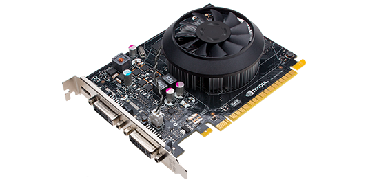
The NVIDIA GeForce GTX 750 Ti is a mid-range desktop graphics card that was announced early 2014. It is based on the first generation of the Maxwell architecture, namely the GM107 chip. Maxwell sets its focus on energy efficiency and was able to outperform the predecessor Kepler and AMD chips in similar performance regions. The GTX 750 Ti supports DirectX 11.2 but only feature level 11_0.
The GeForce GTX 750 Ti is comparable to the Nvidia Geforce GTX 860M for laptops that features the same chip with slightly slower clock rates and therefore also performance.
The 3D performance lies between the Radeon R7 260X and R7 265X from AMD or between the GTX 750 and GTX 660 from Nvidia. In our tests, the 750 Ti was not able to achieve playable framerates in demanding games and highest settings in 1920x1080 (see benchmarks below).
The power consumption as already mentioned is a strong suite for the GTX 750 Ti and it excels the e.g. slightly slower Radeon R7 260X by a great margin (gaming).
NVIDIA GeForce GTX 760
► remove from comparison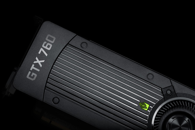
The NVIDIA GeForce GTX 760 is a mid-range desktop graphics card based on the Kepler GK104 chip. It is significantly faster than the mobile Nvidia GeForce GTX 760M for laptops. Depending on the chip temperature and power consumption the core can be clocked between 980-1033 MHz (or even higher). The GDDR5 graphics memory of the 760 is clocked at 3000 MHz (6000 MHz effective).
On average the performance of the GTX 760 is between the GTX 660 and 770 / 680 in the Nvidia lineup and between the Radeon R9 270X and the R9 280 from AMD. The performance is sufficient for maximum detail settings in full HD resolution (for games from 2014 and earlier). However, in some games like Crysis 3 and Thief the average frame rate we tested was only about 30fps (see below).
The power consumption is rated at 160 Watt TDP (load).
| NVIDIA GeForce GTX 750 Ti | NVIDIA GeForce GTX 760 | |||||||||||||||||||
| GeForce GTX 700 Series |
|
| ||||||||||||||||||
| Codename | GM107 | |||||||||||||||||||
| Architecture | Maxwell | Kepler | ||||||||||||||||||
| Pipelines | 640 - unified | 1152 - unified | ||||||||||||||||||
| Core Speed | 1020 - 1085 (Boost) MHz | 980 - 1033 (Boost) MHz | ||||||||||||||||||
| Memory Speed | 2700 MHz | 3000 MHz | ||||||||||||||||||
| Memory Bus Width | 128 Bit | 256 Bit | ||||||||||||||||||
| Memory Type | GDDR5 | GDDR5 | ||||||||||||||||||
| Max. Amount of Memory | 2048 MB | 2048 MB | ||||||||||||||||||
| Shared Memory | no | no | ||||||||||||||||||
| API | DirectX 11.2, Shader 5.0, OpenGL 4.4 | DirectX 11.0, Shader 5.0, OpenGL 4.3 | ||||||||||||||||||
| Power Consumption | 60 Watt | 170 Watt | ||||||||||||||||||
| Transistors | 1.9 Billion | 3.5 Billion | ||||||||||||||||||
| technology | 28 nm | 28 nm | ||||||||||||||||||
| Features | 3D Vision, PhysX, CUDA, GPU Boost 2.0, GeForce Experience, Adaptive VSync | SLI, Purevideo, 3D Vision, PhysX, CUDA, GPU Boost 2.0, GeForce Experience, Adaptive VSync | ||||||||||||||||||
| Date of Announcement | 18.02.2014 | 25.06.2013 | ||||||||||||||||||
| Link to Manufacturer Page | www.nvidia.de | www.nvidia.de |


