

Intel Celeron N5100 vs Intel Celeron N3000 vs Intel Celeron N4500
Intel Celeron N5100
► remove from comparisonThe Intel Celeron N5100 is a quad-core SoC of the Jasper Lake series that is primarily intended for inexpensive notebooks and was announced in early 2021. The four Tremont CPU cores clock between 1.1 and 2.8 GHz (single core Burst) and offer no HyperThreading (SMT). The N5100 uses 1.5 MB L2 and 4 MB L3 cache. The chip is manufactured in 10nm at Intel (most likely in the same process as Ice Lake).
Architecture
The processor architecture is called Tremont and a complete redesign compared to the old Golmont Plus cores in the predecessor. According to Intel, the single thread performance of a core could be improved by 30% on average (10 - 80% in all tests of SPECint and SPECfp).
Features
In addition to the quad-core CPU block, the SoC integrates a 24 EU Intel UHD Graphics GPU clocked from 350 - 800 MHz and a LPDDR4(x) dual channel memory controller (up to 16 GB and 2933 MHz). The chip now also partly integrates Wi-Fi 6 (Gig+), 8 PCIe 3.0 lanes, 14 USB 2.0/ 3.2 ports and two SATA 6.0 ports. The package got bigger and measures 35 x 24 mm (compared to 25 x 24 mm for the N5030 e.g.). The SoC is directly soldered to the mainboard (BGA) and can't be easily replaced.
Performance
While we have not tested a single system powered by the N5100 as of August 2023, it's safe to expect the chip to be 10% to 20% slower than the N6000, as far as multi-thread performance is concerned. In other words, this is a fairly slow processor that is unlikely to make anybody happy.
Power Consumption
Like most other N-class Intel processors, this Celeron has a 6 W default TDP (also known as the long-term power limit). This is rather low; a small metal plate is all it takes to dissipate heat generated by such a CPU.
The Celeron N5100 is manufactured on Intel's first-generation or second-generation [no exact data available] 10 nm process for average, as of early 2023, energy efficiency.
Intel Celeron N3000
► remove from comparison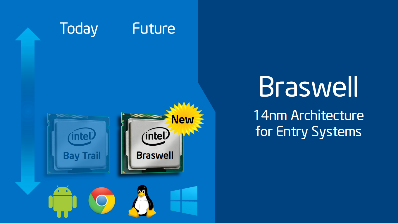
The Intel Celeron N3000 is a low-end dual-core SoC for notebooks, which has been presented in April 2015. It is clocked at 1.04 - 2.08 GHz and part of the Braswell platform. Thanks to its new 14 nanometer low-power process (P1273) with tri-gate transistors, energy efficiency has been significantly improved compared to its predecessor Bay Trail (e.g. Celeron N2840). In addition to the CPU cores, the SoC offers a DirectX 11.2-capable GPU as well as a DDR3L Memory Controller (2x 64 bit, 25.6 GB/s).
Architecture
The processor cores are based on the Airmont architecture, which is basically a slightly modified shrink of the previous Silvermont core. While performance per clock (IPC) has not been improved, the more efficient 14 nm process may lead to a better utilization of the CPU Burst (alias Turbo Boost) and therefore a somewhat higher performance in certain situations.
Performance
Due to only two CPU cores, low clock rates and the weak IPC, the Celeron N3000 is not sufficient for demanding applications and may even struggle on complex websites. Overall, performance is similar to the old Celeron N2810.
Graphics
The HD Graphics (Braswell) is based on the Intel Gen8 architecture, which supports DirectX 11.2 and is also found in the Broadwell series (e.g. HD Graphics 5300). With 12 EUs (Execution Units) and a clock speed of up to 600 MHz, the GPU is significantly faster as the HD Graphics (Bay Trail), but still not powerful enough to handle modern 3D games. The GPU also supports 4K/H.265 video acceleration.
Power Consumption
The entire SoC is rated at an TDP of 4 watts (SDP 3 watts). Thus, the chip can be cooled passively.
Intel Celeron N4500
► remove from comparisonThe Intel Celeron N4500 is a dual-core SoC of the Jasper Lake series that is primarily intended for inexpensive notebooks and was announced in early 2021. The two Tremont CPU cores clock between 1.1 and 2.8 GHz (single core Burst) and offer no HyperThreading. The N4500 uses 1.5 MB L2 and 4 MB L3 cache. The chip is manufactured on the first-gen 10 nm Intel process.
Architecture
The processor architecture is called Tremont and a complete redesign compared to the old Golmont Plus cores in the predecessor. According to Intel, the single thread performance of a core could is up two 30% better on average (10 - 80% in all tests of SPECint and SPECfp).
Features
In addition to the dual-core CPU block, the SoC integrates a 16 EU Intel UHD Graphics GPU clocked from 350 - 750 MHz and a dual-channel DDR4 / quad-channel LPDDR4(x) memory controller (up to 16 GB, up to 2933 MHz). The chip now also partly integrates Wi-Fi 6 (Gig+), 8 PCIe 3.0 lanes, 14 USB 2.0/ 3.2 ports and two SATA 6.0 ports. The package got bigger and measures 35 x 24 mm (compared to 25 x 24 mm for the N5030 e.g.). The SoC is directly soldered to the mainboard (BGA) and can't be easily replaced.
Performance
The average N4500 in our database shapes up to be a fairly slow processor, its multi-thread benchmark scores only just matching those of the Core i3-4010U. (The latter saw the light of day in 2013 as a lower mid-range, dual-core CPU designed for use in ultraportable laptops.) In other words, expect the Celeron to be painfully slow in all but the most basic activities.
You mileage may vary depending on how high the CPU power limits are.
Power consumption
Like most N-class Intel chips, the Celeron has a default TDP (also known as the long-term power limit) of 6 W. This is not much at all and thus good enough for passively cooled tablets, laptops, mini-PCs.
The Celeron N4500 is built with Intel's 2nd generation 10 nm process (not 10 nm SuperFin or Intel 7) for low, as of mid 2023, energy efficiency.
| Model | Intel Celeron N5100 | Intel Celeron N3000 | Intel Celeron N4500 | ||||||||||||||||||||||||||||||||||||||||||||||||||||||||||||||||||||||||||||||||||||
| Codename | Jasper Lake | Braswell | Jasper Lake | ||||||||||||||||||||||||||||||||||||||||||||||||||||||||||||||||||||||||||||||||||||
| Series | Intel Jasper Lake | Intel Celeron | Intel Jasper Lake | ||||||||||||||||||||||||||||||||||||||||||||||||||||||||||||||||||||||||||||||||||||
| Series: Jasper Lake Jasper Lake |
|
|
| ||||||||||||||||||||||||||||||||||||||||||||||||||||||||||||||||||||||||||||||||||||
| Clock | 1100 - 2800 MHz | 1040 - 2080 MHz | 1100 - 2800 MHz | ||||||||||||||||||||||||||||||||||||||||||||||||||||||||||||||||||||||||||||||||||||
| L2 Cache | 1.5 MB | 2 MB | 1.5 MB | ||||||||||||||||||||||||||||||||||||||||||||||||||||||||||||||||||||||||||||||||||||
| L3 Cache | 4 MB | 4 MB | |||||||||||||||||||||||||||||||||||||||||||||||||||||||||||||||||||||||||||||||||||||
| Cores / Threads | 4 / 4 | 2 / 2 | 2 / 2 | ||||||||||||||||||||||||||||||||||||||||||||||||||||||||||||||||||||||||||||||||||||
| TDP | 6 Watt | 4 Watt | 6 Watt | ||||||||||||||||||||||||||||||||||||||||||||||||||||||||||||||||||||||||||||||||||||
| Technology | 10 nm | 14 nm | 10 nm | ||||||||||||||||||||||||||||||||||||||||||||||||||||||||||||||||||||||||||||||||||||
| max. Temp. | 105 °C | 90 °C | 105 °C | ||||||||||||||||||||||||||||||||||||||||||||||||||||||||||||||||||||||||||||||||||||
| Socket | BGA1338 | FCBGA1170 | BGA1338 | ||||||||||||||||||||||||||||||||||||||||||||||||||||||||||||||||||||||||||||||||||||
| Features | DDR4-2933/LPDDR4x-2933 RAM, PCIe 3, GNA, MMX, SSE, SSE2, SSE3, SSSE3, SSE4.1, SSE4.2, VMX, SMEP, SMAP, EIST, TM1, TM2, Turbo, AES-NI, RDRAND, RDSEED, SHA | Intel HD Graphics (Braswell, 12 EUs, 320 - 600 MHz), Wireless Display, Quick Sync, AES-NI, max. 8 GB Dual-Channel DDR3L-1600 (25,6 GB/s), 5x USB 3.0, 4x PCIe 2.0, 2x SATA 6.0 Gbit/s | DDR4-2933/LPDDR4x-2933 RAM, PCIe 3, GNA, MMX, SSE, SSE2, SSE3, SSSE3, SSE4.1, SSE4.2, SMEP, SMAP, EIST, TM1, TM2, Turbo, SST, AES-NI, RDRAND, RDSEED, SHA | ||||||||||||||||||||||||||||||||||||||||||||||||||||||||||||||||||||||||||||||||||||
| iGPU | Intel UHD Graphics (Jasper Lake 24 EU) (350 - 800 MHz) | Intel HD Graphics (Braswell) (320 - 600 MHz) | Intel UHD Graphics (Jasper Lake 16 EU) (350 - 750 MHz) | ||||||||||||||||||||||||||||||||||||||||||||||||||||||||||||||||||||||||||||||||||||
| Architecture | x86 | x86 | x86 | ||||||||||||||||||||||||||||||||||||||||||||||||||||||||||||||||||||||||||||||||||||
| Announced | |||||||||||||||||||||||||||||||||||||||||||||||||||||||||||||||||||||||||||||||||||||||
| Manufacturer | ark.intel.com | ark.intel.com | ark.intel.com | ||||||||||||||||||||||||||||||||||||||||||||||||||||||||||||||||||||||||||||||||||||
| $107 U.S. |

Benchmarks

Average Benchmarks Intel Celeron N5100 → 0% n=0
Average Benchmarks Intel Celeron N4500 → 0% n=0
* Smaller numbers mean a higher performance
1 This benchmark is not used for the average calculation