 Deutsch
 English
 Español
 Français
 Italiano
 Nederlands
 Polski
 Português
 Русский
 Türkçe
 Svenska
 Chinese
 Magyar
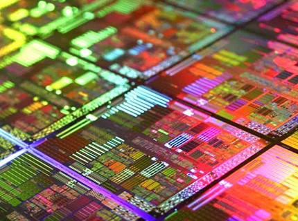
TSMC initiates risk production for its 5 nm node, reveals performance details
As the premier chip-manufacturing foundry that produces SoCs, GPUs and desktop CPUs for many big companies, TSMC is constantly leading the miniaturization race and pushing the technological limits. The Taiwanese company was the first to utilize the 7 nm manufacturing process that helps the current production of chips like Qualcomm’s Snapdragon 855, Huawei’s Kirin 980, and AMDs soon-to-be-released Ryzen 3000 CPUs along with the Radeon VII GPU, plus the upcoming Navi models.
TSMC’s miniaturization roadmaps already include plans to shrink transistors down to 3 nm, but before reaching that level, there is an intermediary 5 nm node, which recently entered its testing period. TSMC together with affiliated IP vendors recently managed to finalize the 5 nm design infrastructure, complete with technology files, process design kits, tools, and flow automations. This enabled the company to already enter 5 nm risk production via multiple silicon test vehicles, with the first 5 nm chips that target high-growth 5G and A.I. markets scheduled to be produced in early 2020.
According to TSMC, preliminary tests conducted on ARM’s Cortex-A72 cores have showed that the upcoming 5 nm process based on the new EUV lithography should provide 1.8X increased logic density and a 15% performance boost over the current 7 nm process. Additionally, the new architecture will allow for SRAM and analog area reductions.
DigiTimes also informs that TSMC is now utilizing 100% of the 7 nm production capacity, as the company has received many new orders from handset manufacturers. Furthermore, TSMC is now transitioning to the EUV lithography process and the first 7 nm chips to use the improved lithography are scheduled to ship in 2H 2019, while the new SoCs for the upcoming iPhone models are expected to be produced throughout Q3 and Q4.
Source(s)
TSMC and OIP Ecosystem Partners Deliver Industry’s First Complete Design Infrastructure for 5nm Process Technology |
Enabling next-generation silicon designs targeting advanced mobile and high-performance computing applications |
Issued by: TSMC Issued on: 2019/04/03 |
| Hsinchu, Taiwan, R.O.C., April 3, 2019—TSMC today announced delivery of the complete version of its 5 nanometer (nm) design infrastructure within the Open Innovation Platform® (OIP). This full release enables 5nm systems-on-chip (SoC) designs in next-generation advanced mobile and high-performance computing (HPC) applications, targeting high-growth 5G and artificial intelligence markets. Leading Electronic Design Automation (EDA) and IP vendors collaborated with TSMC to develop and validate the complete design infrastructure, including technology files, process design kits (PDKs), tools, flows and IP, through multiple silicon test vehicles. TSMC’s 5nm process is already in risk production and offers IC designers a new level of performance and power optimization targeted at the next generation of high-end mobile and HPC applications. Compared with TSMC’s 7nm process, its innovative scaling features deliver 1.8X logic density and 15% speed gain on an ARM® Cortex®-A72 core, along with superior SRAM and analog area reduction enabled by the process architecture. The 5nm process enjoys the benefits of process simplification provided by EUV lithography, and is making excellent progress in yield learning, achieving the best technology maturity at the same corresponding stage as compared to TSMC's previous nodes. TSMC’s comprehensive 5nm design infrastructure includes the full versions of the 5nm Design Rule Manual (DRM), SPICE model, process design kits (PDKs) and silicon-validated foundation and interface IP, and also supports a full range of certified EDA tools and design flows. Backed by the resources of the largest design ecosystem in the industry, TSMC’s Open Innovation Platform®, customers have already started intensive design engagements, paving the way for product tape-outs, pilot activities and early sampling. “TSMC’s 5-nanometer technology offers our customers the industry’s most advanced logic process to address the exponentially growing demand for computing power driven by AI and 5G,” said Cliff Hou, Vice President of Research & Development/Technology Development at TSMC. “5-nanometer technology requires deeper design-technology co-optimization. Therefore, we collaborate seamlessly with our ecosystem partners to ensure we deliver silicon-validated IP blocks and EDA tools ready for customer use. As always, we are committed to helping customers achieve first-time silicon success and faster time-to-market.” 5nm PDKs and EDA Tool Certifications TSMC collaborated with design ecosystem partners, including Cadence, Synopsys, Mentor Graphics, and ANSYS to certify full-line EDA tools through the TSMC OIP EDA Tool Certification Program. The core of the certification program covered silicon-centric EDA tool categories including simulation, physical implementation (Custom Design, APR), timing signoff (STA, Transistor-level STA), Electromigration and IR drop (Gate-level and Transistor-level), physical verifications (DRC, LVS), to RC extractions (RCX). Through the certification program, TSMC and EDA partners enabled design tools to support TSMC 5nm design rules, ensured required accuracy, and improved routability for optimized power, performance and area (PPA) for our customers to take full advantage of TSMC’s 5nm process technology. 5nm Design Flows Foundation IP & 3rd party IP TSMC IP partners also offer interface IP cores supporting both mobile computing and HPC. IP cores such as LPDDR or MIPI PHYs are optimized for mobile solutions, whereas enterprise-dedicated DDR PHYs are optimized for HPC dedicated applications. Other IP cores, such as USB and PCIe PHYs support both segments. These 5nm IP cores are ready for design starts, and IP Silicon reports are available from TSMC and its partners. Availability Partner Quotes “Mentor is proud to once again partner closely with TSMC to enable our mutual customers to quickly design and deliver state-of-the-art ICs using TSMC’s industry-leading 5nm process technology,” said Joe Sawicki, executive vice president for Mentor’s IC Segment. “Our Analog FastSPICE and Calibre physical verification platforms have been in use at the 5nm node with TSMC’s early customers. The same TSMC-certified offerings are now being adopted by companies needing advanced 5nm technology to deliver innovative ICs for the mobile, high-performance computing, automotive, AI and IoT/wearable markets.” “Our strong partnership with TSMC on their 5nm process technology has spanned a broad range of design styles in an effort to successfully push and optimize performance, power and area at low voltage. An early and deep collaboration model, combined with aggressive new R&D innovations in our TSMC-certified digital, signoff and custom/analog products, enables our mutual customers to immediately and confidently engage on high-quality production 5nm design. Using Synopsys’ Fusion Design Platform and DesignWare IP, designers can achieve compressed schedules on their competitive high-performance computing designs targeting the 5G mobile and artificial intelligence markets.” About TSMC TSMC serves its customers with annual capacity of 12 million 12-inch equivalent wafers in 2019 from fabs in Taiwan, the United States, and China, and provides the broadest range of technologies from 0.5 micron plus all the way to foundry’s most advanced processes, which is 7-nanometer today. TSMC is the first foundry to provide 7-nanometer production capabilities and is headquartered in Hsinchu, Taiwan. For more information about TSMC please visit www.tsmc.com. |


