 Deutsch
 English
 Español
 Français
 Italiano
 Nederlands
 Polski
 Português
 Русский
 Türkçe
 Svenska
 Chinese
 Magyar
Nvidia CEO Jensen Huang unveils unified 7 nm Ampere GPU architecture pre GTC 2020 keynote, no details on the next gen RTX 3000 gaming GPUs, unfortunately
Everyone was expecting Jensen Huang to tease something about the Apmere-based GeForce RTX 3000 gaming GPUs in the rescheduled GTC 2020 keynote. Unfortunately, Huang did not mention anything about the upcoming gaming GPUs, but he did specify that the Ampere microarchitecture will be used for all next gen GPUs. This means that the GeForce gaming GPUs and the Quadro professional GPUs will from now on be based on the same tech integrated in data center cards like the A100 HPC GPU unveiled during the keynote. Of course, the processing power will be scaled down for the consumer products, as Huang explained that "there’s great overlap in the architecture, but not in the configuration."
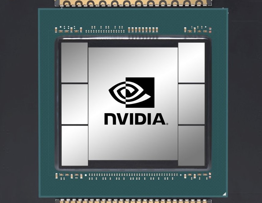
The new A100 GPU is made of 54 billion transistors using an advanced 3D packaging technology called CoWoS (chip on wafer on substrate), which puts the HBM2 memory on the same substrate as the chip, providing 1.6 TB/s of framebuffer bandwidth. With the new chip, Nvidia now includes the third generation of Tensor Cores that have a new numerical format called Tensor Float 32 (TF32) replacing the FP32. In addition to normal floating point acceleration, the new chip is able to accelerate sparsity-based operations. Thanks to the new Multi-instance GPU (MIG) design, the theoretical throughput of the new A100 chip is up to seven times higher than that of the current V100 chips. Nvidia will be offering eight A100 GPUs combined in one DGX A100 node able to muster a peak performance of 5 petaflops of compute performance for US$200,000.
Even though the Ampere-based gaming GPU specs remain a mystery, Nvidia's detailed Ampere microarchitecture in-depth analysis blog post does mention that all upcoming GPUs will offer third gen NVLink integration, plus we get confirmation that Ampere is offering PCIe Gen 4 support. Nvidia will probably wait for AMD to announce the RDNA2 gaming GPUs first (most likely happening in Q3 this year) and then crush all hopes and dreams with a swift Ampere-based GeForce RTX 3000 counterattack.


