Deutsch
 English
 Español
 Français
 Italiano
 Nederlands
 Polski
 Português
 Русский
 Türkçe
 Svenska
 Chinese
 Magyar
Intel shows off a 10nm wafer and a bevy of other developments on the occasion of Technology and Manufacturing Day
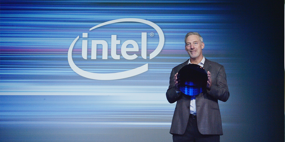
Intel celebrated its Technology and Manufacturing Day in Beijing, China, yesterday and used the occasion to deliver key updates on its developmental roadmap. Intel's group president of Manufacturing, Operations and Sales, Stacy Smith, re-iterated that Intel's manufacturing process is advancing in accordance with Moore's Law and that Moore's Law is not ending anytime soon. For those not in the know, Moore's Law was first propounded by Intel co-founder Gordon Moore in 1965. It states that the number of transistors and resistors on an integrated circuit doubles approximately every two years. The current doubling rate is approximately 18 months. Mr. Smith said Intel has a three-year lead in process technology and is the main driver of Moore's Law.
Intel Senior Fellow, Mark Bohr presented the salient features of the 10nm process. Intel's 10nm process has currently the world's tightest transistor and metal pitches, with over 100 million transistors per mm2. Just like the current 14nm process, the 10nm family will sport a triplet of 10nm, 10nm+, and 10nm++ processes. The 10nm 'Cannon Lake' wafer was displayed during the presentation for the first time. The new 10nm process will also power the demands of enterprises and data centers. Upcoming field-programmable gate arrays (FPGAs, codenamed 'Falcon Mesa') will employ the 10nm++ process and are poised to power data centers, wireless 5G, network function virtualization (NFV), and many industrial applications. ARM SoC will soon be developed using Intel's 10nm process with performance north of the 3GHz mark. Intel showed off a 10nm wafer containing ARM Cortex A-75 cores.
Finally, Intel said that it will be shipping the first 64-layer triple level cell (TLC) 3D NAND SSD targeted towards datacenters. Top-tier cloud service providers have already been testing the new TLC 3D NAND SSDs since August this year and Intel will soon make the product available for data centers by year end.
Source(s)