 Deutsch
 English
 Español
 Français
 Italiano
 Nederlands
 Polski
 Português
 Русский
 Türkçe
 Svenska
 Chinese
 Magyar
AMD: The upcoming "Carrizo" APU generation casts its shadow before
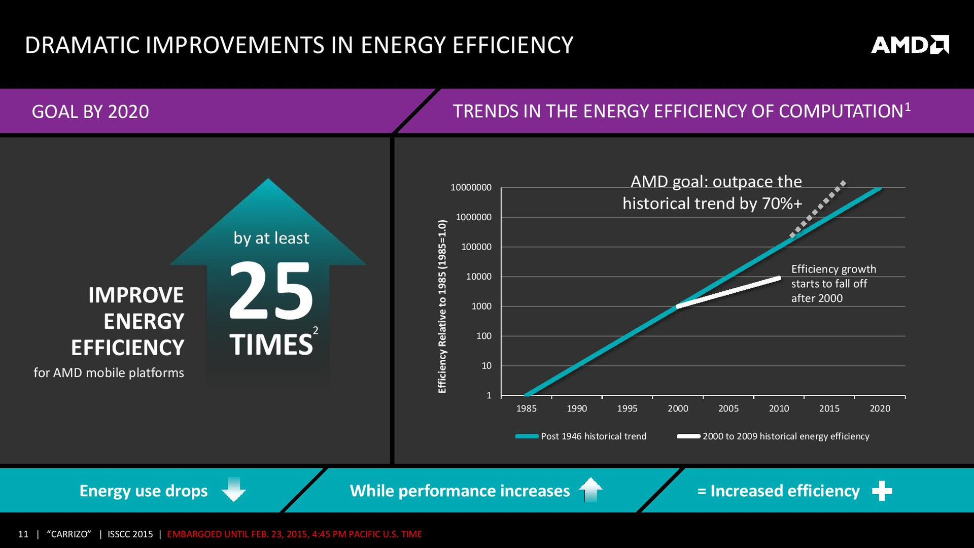
On paper, AMD is currently facing a difficult situation: While their big rival Intel can use the highly advanced 14 nm lithography since several months, they still produce their APUs in 28 nm technology. This is a big disadvantage in a product class which almost exclusively depends on energy efficiency. AMDs promises for the upcoming "Carrizo" APU are all the more impressive.
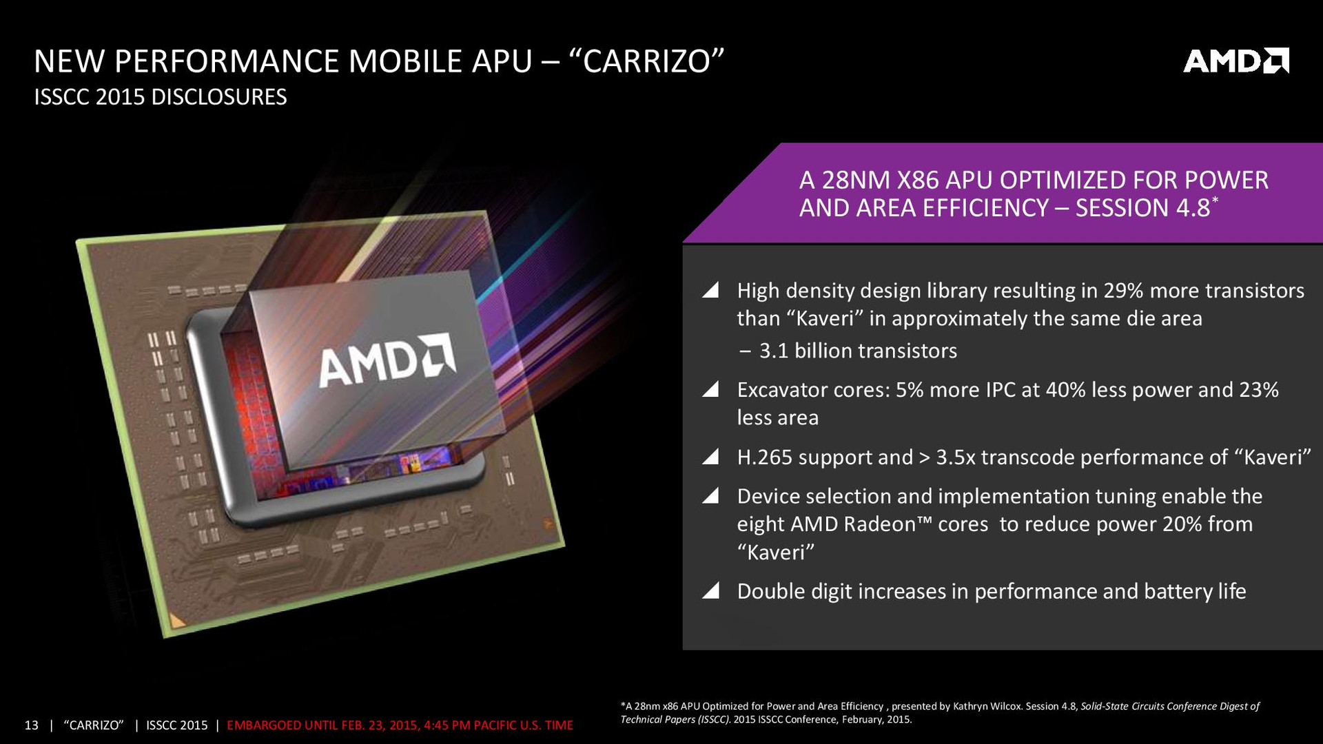
Before dealing with efficiency, we will give a general overview of Carrizo. At the first glance, the technical specs did not change greatly: Apart from the lithography, also the number of CPU cores (4 cores, 2 modules) and GPU clusters (8 compute cores, 512 shaders) remained the same. What is new is the complete integration of the Southbridge. As a result Carrizo can be considered a "genuine" mid-range SoC (In Intel's Broadwell architectures, the chipset only sits besides the processor on the same board). Thus, Carrizo and Carrizo-L (successor of the Beema platform) could possibly use the same board infrastructure in the future, which would decrease integration cost of the notebook manufacturer.
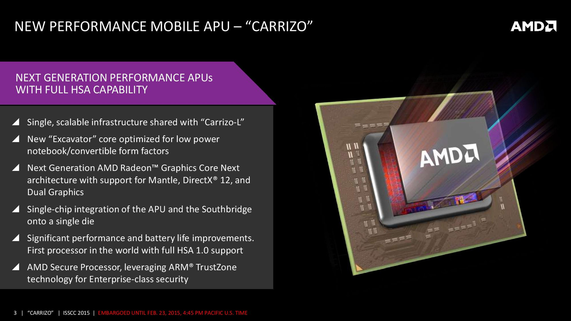
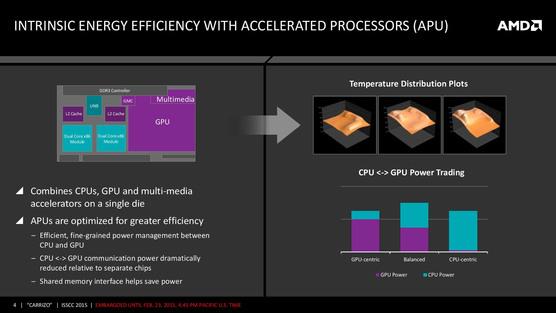
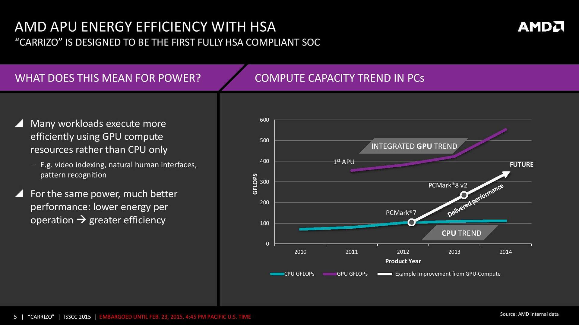
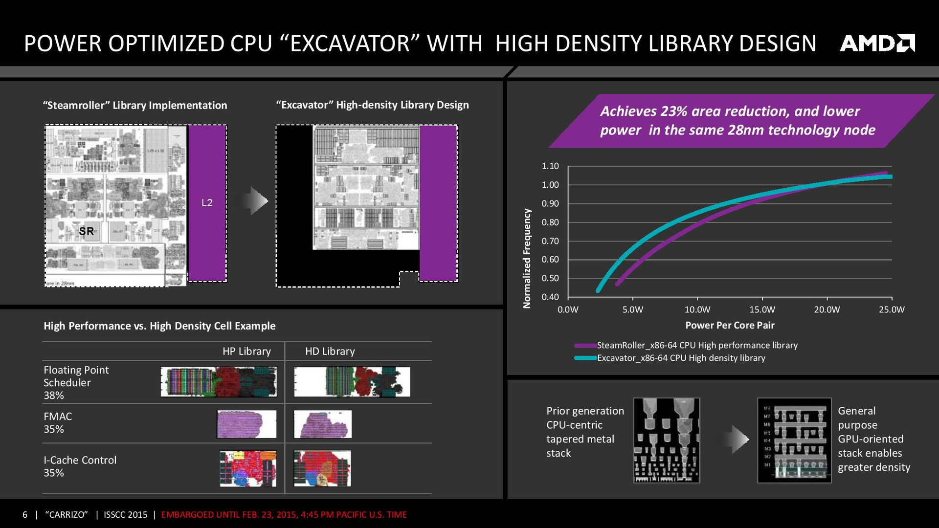
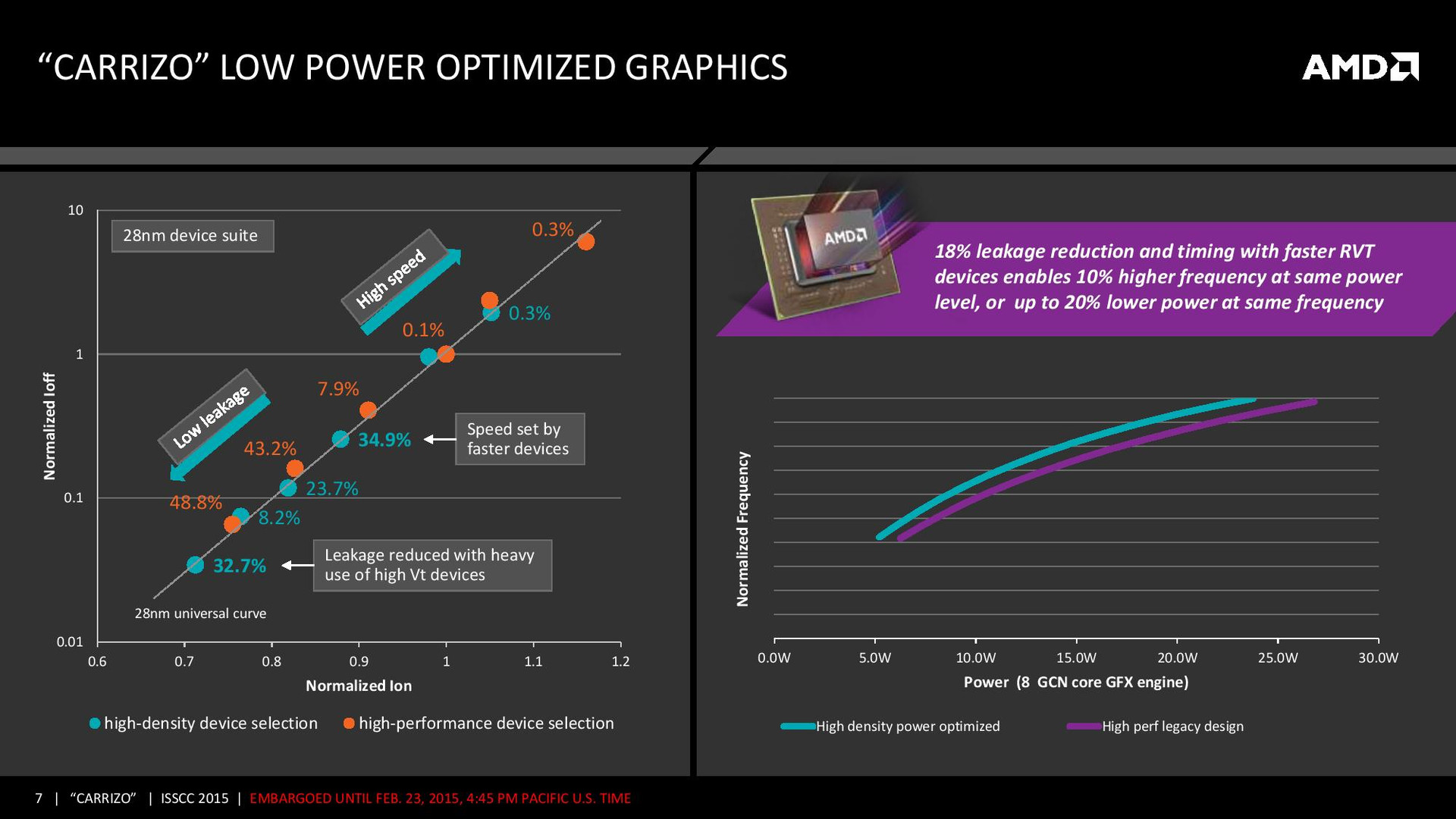
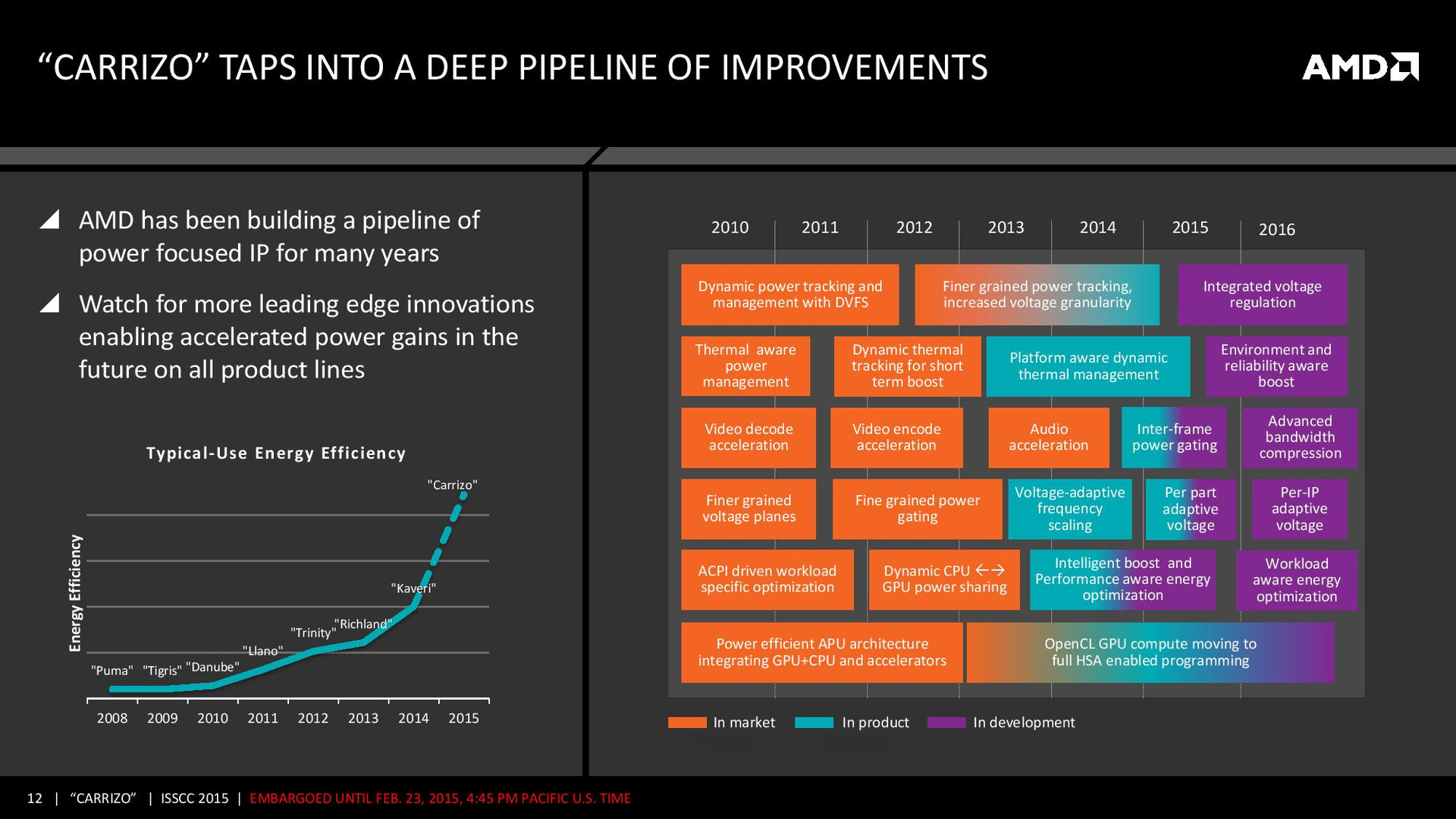
In order to free space for the I/O part and other improvements, AMD tried to increase the packing density, i.e. the number of transistors per mm². Successfully: Thanks to their experiences in the GPU range, where packing density is already highly important for some time and the use of special high-density libraries, the size of the CPU cores could be reduced by 23 percent. Simultaneously the power consumption even fell by 40 percent. In addition, AMD promises that the new Excavator cores' performance per MHz will be 5 percent higher than the Steamroller/Kaveri's. The graphics core also profits from small improvements. It should need 20 percent less energy at the same clock rate (or clock 10 percent higher with the same power consumption). As a result, it could be the first time a ULV model features 512 active shader units.
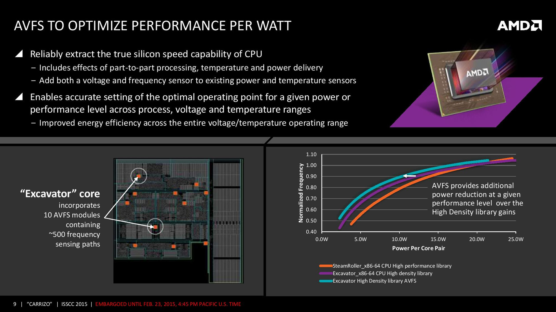
Another particularly innovative technology for improving the energy efficiency is called Voltage Adaptive Operation. It is basically based on the fact, the all CPUs are generally driven by a higher voltage than necessary because of unavoidable voltage fluctuations. Instead of using this inefficient precaution, Carrizo permanently monitors the supply voltage and reduces the clock rate for a short time when it falls. In this way, the chip also works stable with lower voltage. The strategy of the so-called Adaptive Voltage and Frequency Scaling (AVFS) is similar. It should bring improvements in adjusting clock and voltage to current temperature and quality of a particular chip.

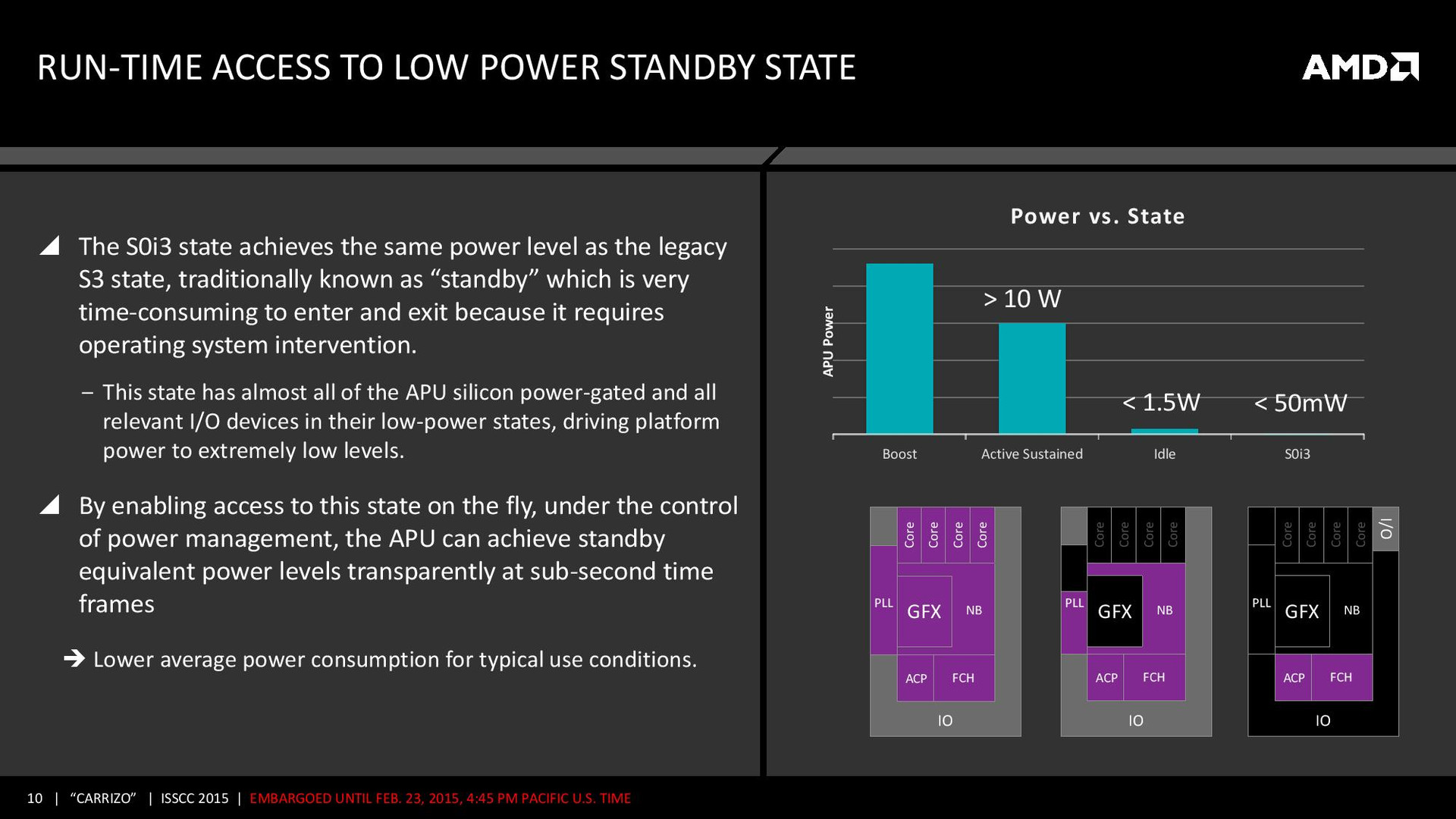
Overall, AMD promised that performance as well as battery life will improve by a two-digit number with Carrizo, which is more than double that complex as a typical Broadwell chip (2C + GT2 1.3 billion transistors) with 3.1 billion transistors. Further buying incentives are the updated video unit (H.265-/HEVC support, 3.5 x transcoding performance) and a particularly fast and frugal standby mode called S0i3. So far, the manufacturer did not reveal the model range and the exact release date. At the present, we assume that it will launch during the Computex in early June.
Source(s)
Eigene
